






Opens in a new tab

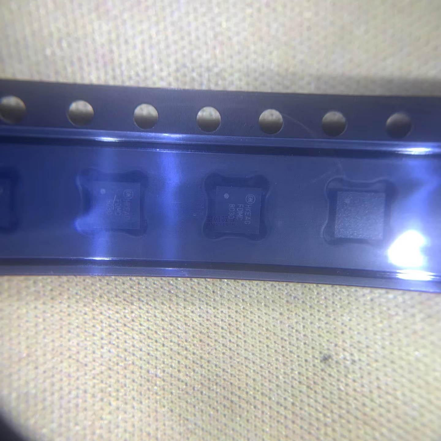
FDMC8030

N-channel MOSFET, 30V 11A, RDS(on) 11mΩ@10V, PowerTrench, DFN-8 3.3×3.3mm, onsemi FDMC8030

5400

Effective Inventory

Image for reference only

Manufacturer Part:

FDMC8030

Package:

DFN-8 (Dual Flat No-lead, 8 pins), 3.3mm × 3.3mm × 0.8mm, exposed pad, tape and reel

Brand:

Quality Commitment

Shipping & Payment

Service & Packaging

Product Manual

Description

Product Overview

The FDMC8030 is an N-channel enhancement mode power MOSFET from ON Semiconductor, featuring PowerTrench® technology for high performance in a compact DFN-8 package. This device is rated for 30 V drain-source voltage and 11 A continuous drain current (at 25°C), with extremely low on-resistance RDS(on) of 11 mΩ maximum at VGS = 10 V and 14 mΩ maximum at VGS = 4.5 V. The PowerTrench MOSFET technology delivers fast switching speed, low gate charge (11 nC typical), low output capacitance, and high power density — optimizing efficiency in high-frequency switching applications. Housed in an 8-pin DFN package (3.3mm × 3.3mm), the FDMC8030 offers excellent thermal performance in a small footprint, making it ideal for DC-DC converters, load switches, motor drives, battery management systems, power management, and other high-efficiency power applications.

Key Specifications

Parameter Value
Manufacturer ON Semiconductor (onsemi)
Part Number FDMC8030
Product Type N-Channel Enhancement Mode Power MOSFET
Technology PowerTrench® MOSFET
Drain-Source Voltage (VDS) 30 V
Gate-Source Voltage (VGS) ±20 V
Continuous Drain Current (ID) 11 A @ 25°C; 8.5 A @ 100°C
Pulsed Drain Current (IDM) 44 A
Drain-Source On-Resistance (RDS(on)) 11 mΩ max @ VGS = 10V, ID = 11A
RDS(on) @ 4.5V 14 mΩ max @ VGS = 4.5V, ID = 8.5A
Gate Threshold Voltage (VGS(th)) 1.5 V typical (0.9V~2.0V range)
Total Gate Charge (Qg) 11 nC typical @ VGS = 10V
Gate-Drain Charge (Qgd) 3.5 nC typical
Gate-Source Charge (Qgs) 2.5 nC typical
Input Capacitance (Ciss) 850 pF typical @ VDS = 15V, VGS = 0V
Output Capacitance (Coss) 230 pF typical
Reverse Transfer Capacitance (Crss) 95 pF typical
Body Diode Forward Voltage 0.85 V typical @ IS = 11A
Diode Reverse Recovery Time (trr) Fast body diode
Total Power Dissipation (PD) 2.5 W @ 25°C (DFN-8 package)
Thermal Resistance (Junction to Ambient) RθJA ≈ 50°C/W (on standard PCB)
Thermal Resistance (Junction to Pad) RθJC ≈ 4°C/W
Maximum Junction Temperature +175°C
Operating Temperature Range -55°C ~ +175°C
Package / Case Style DFN-8 (Dual Flat No-lead, 8 pins)
Package Dimensions 3.3 mm × 3.3 mm × 0.8 mm (approximate)
Mounting Type Surface Mount (SMD / SMT)
RoHS RoHS Compliant / Lead-free
Halogen Free Yes
Packaging Tape and reel
Product Status Active

Features

  • N-channel enhancement mode power MOSFET
  • PowerTrench® technology for high performance
  • 30 V drain-source voltage rating
  • 11 A continuous drain current @ 25°C
  • Ultra-low on-resistance: 11 mΩ @ VGS=10V
  • 4.5 V gate drive capability (14 mΩ @ 4.5V)
  • Low gate charge: 11 nC typical
  • Fast switching speed
  • High power density in compact package
  • Fast body diode with low recovery
  • 850 pF input capacitance
  • 230 pF output capacitance
  • Exposed DFN pad for excellent thermal
  • 3.3mm × 3.3mm DFN-8 package
  • 2.5 W power dissipation @ 25°C
  • High 175°C junction temperature rating
  • RoHS compliant / lead-free
  • Halogen free
  • Tape and reel packaging
  • Ideal for high-efficiency DC-DC converters

Applications

  • DC-DC converters (buck, boost, synchronous rectifiers)
  • Load switches and power distribution
  • Battery management systems (BMS)
  • Motor drives and motor control
  • Power management IC (PMIC) companion
  • Portable electronics and computing
  • LED drivers and lighting
  • Server and telecom power systems
  • Switch mode power supplies (SMPS)
  • High-efficiency power switching
Product Introduction: FDMC8030 Product Introduction

The FDMC8030 is an N-channel enhancement mode power MOSFET from ON Semiconductor’s PowerTrench® family, designed for high-efficiency power switching applications in consumer, computing, and industrial electronics. PowerTrench technology is ON Semi’s advanced trench MOSFET architecture that delivers an optimized combination of low on-resistance (RDS(on)), low gate charge (Qg), low output capacitance (Coss), and fast switching speed — all critical parameters for achieving high efficiency in high-frequency power conversion. The FDMC8030 is rated for 30 V drain-source voltage and 11 A continuous drain current at 25°C, derated to 8.5 A at 100°C junction temperature. Its low on-resistance of 11 mΩ maximum at 10 V gate drive and 14 mΩ maximum at 4.5 V gate drive enables low conduction losses, while the low gate charge of 11 nC typical minimizes switching losses — an important balance for overall efficiency in DC-DC converter applications. The 4.5 V gate drive capability makes the device suitable for both 5 V and 12 V gate drive systems commonly found in computing and telecom power applications. The DFN-8 package (3.3 mm × 3.3 mm) provides an excellent combination of compact size and thermal performance. The exposed bottom pad of the DFN package provides a low thermal resistance path from the die to the PCB, enabling effective heat dissipation and allowing the device to handle its rated power in a small footprint. With 8 pins (multiple source and drain connections), the package also provides multiple parallel current paths for lower package resistance and improved current distribution. Key features include a fast body diode with low reverse recovery charge, which is important for synchronous rectifier and half-bridge applications where the body diode conducts during dead time. The device is fully characterized for both static and dynamic parameters including capacitances, gate charge characteristics, switching times, and safe operating area (SOA). With an operating temperature range of -55°C to +175°C and a high junction temperature rating of 175°C, the FDMC8030 provides substantial thermal headroom for demanding applications. RoHS compliant, lead-free, and halogen-free, it is packaged in tape and reel for high-volume automated assembly. Overall, the FDMC8030 is a versatile 30V N-channel MOSFET that finds application in DC-DC converters, load switches, battery management, motor drives, and power management circuits where high efficiency and small size are required.

Working Principle: FDMC8030 Working Principle

The FDMC8030 is an N-channel enhancement mode MOSFET (Metal-Oxide-Semiconductor Field-Effect Transistor) that operates as a voltage-controlled switch. In an N-channel MOSFET, current flows between the drain and source terminals through a channel of N-type semiconductor material, and the conductivity of this channel is controlled by the voltage applied to the gate terminal. The gate is electrically insulated from the channel by a thin layer of silicon dioxide (the ‘oxide’ in MOSFET), so the gate draws essentially zero DC current — only a small charging current when switching. In enhancement mode, the channel is normally non-conducting (off) when the gate-source voltage (VGS) is 0 V. When a positive VGS is applied that exceeds the gate threshold voltage (VGS(th), typically 1.5 V for FDMC8030), an electric field forms between the gate and the semiconductor, attracting electrons to the region under the gate oxide and creating a conductive N-type channel between the drain and source. The higher the VGS above threshold, the wider and more conductive the channel becomes, resulting in lower on-resistance (RDS(on)). ON Semiconductor’s PowerTrench technology uses a trench (vertical) gate structure rather than a planar (horizontal) structure. In the trench structure, the gate electrode is formed in a trench etched vertically into the silicon, with the gate oxide lining the trench walls. This vertical structure has several advantages: the channel is formed along the vertical trench walls, which increases the effective channel width per unit of die area (reducing RDS(on) for a given die size); the gate-to-drain overlap capacitance (Crss) is reduced, improving switching speed and reducing switching losses; and the overall die can be smaller for a given RDS(on) rating, reducing cost. When the MOSFET is fully on (saturated, with VGS well above threshold), it behaves like a low-value resistor (RDS(on)), and power dissipation is I² × RDS(on). This is the conduction loss. When switching between on and off states, energy is dissipated as the voltage and current transition — these are the switching losses, which depend on gate charge, output capacitance, and switching frequency. The FDMC8030’s low gate charge and low output capacitance minimize these switching losses, which is particularly important in high-frequency DC-DC converter applications. The body diode (also called the parasitic diode or intrinsic diode) is formed by the body-drain PN junction inherent in the MOSFET structure. It conducts when the drain-source voltage goes negative (for an N-channel device), and its characteristics are important in synchronous rectifier and bridge applications where the body diode carries current during dead time. The fast body diode of the FDMC8030 reduces losses in these applications. Overall, the PowerTrench architecture provides an optimal balance of low conduction loss, low switching loss, and high power density.

Pin Description: FDMC8030 Pin Definition and Functions

The FDMC8030 is an N-channel power MOSFET in an 8-pin DFN (Dual Flat No-lead) surface-mount package with exposed thermal pad.

Pin Designation Description
Pins 1-4 Gate (G) + NC Pin 4 is Gate; Pins 1-3 are typically No Connect or source in DFN-8
Pins 5-8 Drain (D) Multiple drain pins connected together for high current
Exposed Pad Source (S) Large exposed pad on bottom = Source connection (also for thermal)

Note: In typical DFN-8 power MOSFET pinouts, one side contains the gate pin(s), the opposite side contains multiple drain pins, and the large exposed bottom pad serves as both the source connection and the primary thermal path. Exact pin assignments should be verified against the official datasheet.

Package Features:

  • Package Style: DFN-8 (Dual Flat No-lead, 8 connections)
  • Package Dimensions: 3.3 mm × 3.3 mm × 0.8 mm (approximate)
  • Exposed Thermal Pad: Yes (large bottom pad for heat dissipation)
  • Termination: Tin-plated, lead-free
  • Mounting: Surface mount technology (SMT)
  • Thermal Resistance (Junction to Case): ~4°C/W (excellent thermal performance)
  • Current Handling: Multiple drain and source connections for low resistance
  • Packaging: Tape and reel (standard for SMT assembly)
  • Weight: Lightweight
  • RoHS Compliant: Yes
  • Halogen Free: Yes

Application Notes:

  • Use wide copper traces on drain and source for low resistance and good heat spreading
  • Maximize copper area on the source pad for thermal dissipation
  • Place gate resistor close to the gate pin for damping and noise immunity
  • Ensure adequate PCB thermal vias under the exposed pad
  • Refer to the ON Semiconductor FDMC8030 datasheet for exact pinout, dimensions, recommended PCB footprint, and thermal design guidelines
Application Scenarios: In which products and applications is FDMC8030 used
  • DC-DC Converters: Used as the control switch or synchronous rectifier in buck, boost, buck-boost, and other DC-DC converter topologies in computing, telecom, and consumer electronics, where the low RDS(on) and low gate charge combine for high efficiency across light and heavy load conditions
  • Load Switches & Power Distribution: Deployed as high-side or low-side load switches in portable electronics, servers, and communication equipment for power distribution, enabling and disabling power rails to subsystems, and providing protection features like current limiting and voltage monitoring
  • Battery Management Systems (BMS): Used in battery management systems for Li-ion battery packs (laptops, power tools, e-bikes, EV modules) as discharge/control FETs, cell balancing switches, and protection circuit switches, leveraging the 30V rating for multi-cell battery stacks
  • Motor Drives & Motor Control: Found in BLDC and brushed DC motor drive circuits for power tools, robotics, drones, and automotive actuators, where high current capability and efficient switching contribute to extended battery life and high performance
  • Power Management IC Companions: Used alongside power management ICs (PMICs) as external pass transistors for high-current power rails, or as additional switching regulators controlled by the PMIC’s PWM outputs
  • Portable Electronics & Computing: Used in laptops, tablets, smartphones (high-power variants), wearables, and accessories for efficient power conversion, battery charging, and power management in space-constrained designs where the small DFN-8 package is essential
  • LED Drivers & Lighting: Deployed in LED driver circuits for general lighting, automotive lighting, and display backlighting as the switching element in buck, boost, and buck-boost LED driver topologies, providing efficient constant-current drive for LED arrays
  • Server & Telecom Power: Used in server power supplies, telecom rectifiers, and datacom equipment for intermediate bus converters, point-of-load regulators, and power OR-ing applications where efficiency and power density are critical design requirements
Alternative Models: What chips are recommended as replacements for FDMC8030
Part Number Manufacturer VDS ID @25°C RDS(on) max Package
FDMC8030 ON Semi 30V 11A 11mΩ @ 10V DFN-8 (3.3×3.3)
FDMC8420 ON Semi 30V 17A 7.6mΩ @ 10V DFN-8 (3.3×3.3)
FDV301N ON Semi 25V 2.5A 80mΩ @ 4.5V SOT-23
SI7134DP Vishay 30V 12A 10.5mΩ @ 10V PowerPAK SO-8
AO3400A Alpha & Omega 30V 5.8A 25mΩ @ 10V SOT-23-3L
IRLML6246TRPBF Infineon 20V 16A 7.2mΩ @ 4.5V TSOP-6

Recommend Parts

ISL95855HRTZ-T

IMVP8 3+2+1 phase buck controller, R3 technology, 4.5-25V input, 48-TQFN

Brand: Renesas

Package: 48-TQFN (6×6 mm, exposed pad)

IN STOCK: 2156pcs

Cargo cycle: 3-7 Days

The minimum order is 1

IRFB4019PBF

150V N-Channel HEXFET Power MOSFET, 47A, 34 mΩ RDS(on), TO-220AB

Brand: infineon

Package: TO-220AB

IN STOCK: 2409pcs

Cargo cycle: 3-7 Days

The minimum order is 1

NRF52832-QFAA-T

Nordic BLE SoC, ARM Cortex-M4 @ 64MHz, 64KB Flash, 32KB RAM, QFN-48

Package: See datasheet

IN STOCK: 10958pcs

Cargo cycle: 3-7 Days

The minimum order is 1

UCC28740DR

CVCC Flyback Controller, 700V startup, opto feedback, <10mW no-load, SOIC-7

Brand: TI

Package: SOIC-7 (4.9 x 3.9 x 1.75 mm)

IN STOCK: 4840pcs

Cargo cycle: 3-7 Days

The minimum order is 1

MMUN2211LT1G

NPN digital transistor, R1=10kΩ R2=10kΩ, 50V, 100mA, SOT-23-3, pre-biased BRT switch

Brand: Onsemi

Package: SOT-23-3 (TO-236, SC-59)

IN STOCK: 8500pcs

Cargo cycle: 3-7 Days

The minimum order is 1

PIC32MX795F512L-80I/PF

32-bit PIC32MX MCU with Ethernet/CAN/USB, 80MHz, 512KB Flash, TQFP-100, industrial

Brand: MICROCHIP

Package: TQFP-100 (14 x 14 mm)

IN STOCK: 7912pcs

Cargo cycle: 3-7 Days

The minimum order is 1





