






Opens in a new tab

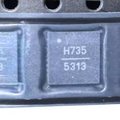
HMC735LP5E

GaAs InGaP HBT MMIC VCO, 10.5-12.2GHz, +17dBm Pout, -100dBc/Hz phase noise @100kHz, divide-by-4 output, 5V supply, 32-QFN 5x5mm, ADI Hittite X-band.

1520

Effective Inventory

Image for reference only

Manufacturer Part:

HMC735LP5E

Package:

32-Lead QFN (5mm x 5mm w/ EP)

Quality Commitment

Shipping & Payment

Service & Packaging

Product Manual

Description

Product Overview

The HMC735LP5E is a high-performance GaAs InGaP Heterojunction Bipolar Transistor (HBT) MMIC Voltage Controlled Oscillator (VCO) from Analog Devices (formerly Hittite Microwave), operating in the X-band frequency range of 10.5 to 12.2 GHz. As a fully integrated monolithic VCO, the device incorporates resonators, negative resistance devices, varactor diodes, and a divide-by-4 prescaler output, eliminating the need for external resonator components. The monolithic construction ensures excellent phase noise performance and exceptional stability over temperature, mechanical shock, and process variations. The main RF output delivers +17 dBm typical output power from a +5V supply, while the divide-by-4 output provides a 2.625 to 3.05 GHz signal suitable for PLL feedback or lower frequency reference. The prescaler can be disabled to conserve approximately 100 mA of supply current when not needed. Packaged in a compact 32-lead 5×5 mm QFN with exposed pad for thermal management, the HMC735LP5E requires no external matching components and is specified over the commercial-industrial temperature range of -40 degrees C to +85 degrees C. The E suffix denotes RoHS-compliant construction with matte tin lead finish.

Key Specifications

Parameter Min. Typ. Max. Units
Frequency Range (Fo) 10.5 — 12.2 GHz
Frequency Range (Fo/4) 2.625 — 3.05 GHz
Output Power (RFOUT) 14 17 — dBm
Output Power (RFOUT/4) — -8 — dBm
SSB Phase Noise @ 100 kHz offset — — -100 dBc/Hz
Tuning Voltage Range (VTUNE) 1 — 15 V
Supply Voltage (Vcc) 4.75 5.0 5.25 V
Supply Current (Total) — 180 217 mA
Second Harmonic — -18 — dBc
Third Harmonic — -40 — dBc
Subharmonic (1/2) — -65 — dBc
Frequency Pulling (2:1 VSWR) — 50 — MHz p-p
Frequency Pushing — 30 — MHz/V
Technology GaAs InGaP HBT MMIC —
Package 32-Lead QFN, 5mm x 5mm w/ exposed pad —
MSL Rating MSL3 —
Operating Temperature -40 — +85 degrees C
RoHS Compliance Yes (E suffix) —

Features

  • Wide tuning range: 10.5 GHz to 12.2 GHz (X-band)
  • Dual outputs: main RF (Fo) and divide-by-4 (Fo/4 = 2.625-3.05 GHz)
  • High output power: +17 dBm typical from +5V supply
  • Excellent phase noise: -100 dBc/Hz at 100 kHz offset
  • GaAs InGaP HBT monolithic microwave IC technology
  • Fully integrated resonator – no external components needed
  • Integrated varactor diodes for voltage tuning
  • Divide-by-4 prescaler with enable/disable for power saving
  • Prescaler disable saves ~100 mA supply current
  • No external matching components required
  • Monolithic structure ensures excellent stability over temperature and shock
  • Low harmonic and subharmonic content
  • Compact 32-lead 5×5 mm QFN package (25 mm2 footprint)
  • Exposed pad for thermal management
  • Compatible with surface mount manufacturing techniques
  • MSL3 moisture sensitivity rating
  • RoHS compliant with matte tin finish (HMC735LP5E)
  • Industrial temperature range: -40C to +85C
  • Supported by ADIsimPLL simulation tool
  • Evaluation board available (110227-HMC735LP5)

Applications

  • Point-to-point and point-to-multipoint microwave radios
  • Test equipment and industrial controls
  • SATCOM and VSAT satellite communications
  • Military and aerospace end-use applications
  • Local oscillator (LO) for upconverters and downconverters
  • PLL frequency synthesis with external PLL IC
  • X-band radar and electronic warfare systems
  • Phased array beam steering systems
  • Signal generators and frequency sources
  • Broadband communication infrastructure

Product Introduction: HMC735LP5E Product Introduction

The HMC735LP5E is a high-performance monolithic microwave integrated circuit (MMIC) voltage controlled oscillator (VCO) from Analog Devices Hittite microwave product line. Fabricated using GaAs InGaP heterojunction bipolar transistor (HBT) technology, this X-band VCO covers a frequency range of 10.5 to 12.2 GHz with a tuning voltage range of 1V to 15V. What sets the HMC735LP5E apart from discrete VCO solutions is its complete monolithic integration: all critical components including the resonator, negative resistance active devices, varactor diodes, and output buffer amplifiers are fabricated on a single GaAs die. This monolithic construction delivers several key advantages: exceptional phase noise performance that remains consistent over temperature, mechanical shock, and process variations; no external resonator components required; and minimal frequency pulling due to load impedance changes. The VCO provides two output signals: the main RF output at the fundamental frequency (Fo = 10.5-12.2 GHz) delivering +17 dBm typical output power, and a divide-by-4 output (Fo/4 = 2.625-3.05 GHz) that is ideal for use as a PLL feedback signal or as a lower frequency reference output. The prescaler can be disabled when not needed, reducing total supply current by approximately 100 mA for power-sensitive applications. The main output buffer provides excellent load pulling performance of only 50 MHz peak-to-peak into a 2:1 VSWR, ensuring frequency stability even when driving mismatched loads. The HMC735LP5E operates from a single +5V supply with a typical total supply current of 180 mA (217 mA max). Housed in a compact 32-lead 5×5 mm QFN package with an exposed thermal pad for efficient heat dissipation, the device requires no external matching components, significantly simplifying board design and reducing overall solution footprint. The E suffix version is RoHS compliant with 100% matte tin lead finish and MSL3 rating.

Working Principle: HMC735LP5E Working Principle

The HMC735LP5E is a voltage controlled oscillator based on a negative-resistance topology implemented in GaAs InGaP HBT technology. The core of the VCO consists of a pair of HBT transistors configured in a cross-coupled or Colpitts-style negative resistance configuration that compensates for the losses in the resonant tank circuit. The resonant tank is formed by integrated transmission line resonators and varactor diodes. The varactor diodes are semiconductor devices whose capacitance varies with applied reverse bias voltage – as the tuning voltage (VTUNE) increases, the varactor capacitance decreases, raising the resonant frequency of the tank circuit, and vice versa. This voltage-dependent tuning allows the oscillator frequency to be electronically controlled over the 10.5 to 12.2 GHz range. The negative resistance from the active devices cancels the equivalent parallel resistance of the tank, sustaining oscillation at the resonant frequency. Since all resonator elements are monolithically integrated on the same GaAs substrate, the VCO exhibits excellent phase noise and frequency stability – there are no external components to introduce noise or mechanical instability. The oscillator signal is buffered by an amplifier stage that provides isolation between the VCO core and the load, minimizing frequency pulling effects caused by load impedance variations. This buffer also delivers the +17 dBm output power. A separate divide-by-4 prescaler circuit takes a portion of the main VCO signal and divides it by four, producing a lower frequency output at Fo/4. This divider is implemented with digital logic and can be powered down by leaving the Vcc(Dig) pin open, saving approximately 100 mA of supply current. The divide-by-4 output is particularly useful in PLL applications as it provides a lower frequency signal that can be directly compared with a reference frequency in a phase-frequency detector, eliminating the need for an external prescaler. The thermal management is handled through the exposed ground paddle on the bottom of the QFN package, which must be soldered to the PCB ground plane to provide both a low-inductance RF ground and a low-thermal-resistance path for heat dissipation.

Pin Description: HMC735LP5E Pin Definition and Functions
Pin(s) Function Description
4 RFOUT/4 Divide-by-4 output. Requires external DC blocking capacitor. Output level: -8 dBm typical.
6 Vcc (Dig) Supply voltage for the prescaler (divide-by-4) circuit. Connect to +5V. If prescaler is not needed, this pin may be left open to conserve approximately 100 mA of current.
19 RFOUT Main RF output at fundamental frequency (10.5-12.2 GHz). AC coupled. Output power: +17 dBm typical. Requires external 50 ohm termination and DC block.
21 Vcc (RF) RF output stage supply voltage, +5V. Bypass with 100 pF, 1000 pF, and 2.2 uF capacitors to ground.
29 VTUNE Oscillator control voltage and frequency modulation input. Tuning range: 1V to 15V. Modulation bandwidth depends on drive source impedance.
5, 11, 18 GND Ground pins. Must be connected to RF/DC ground plane with low inductance vias.
Paddle (bottom) GND / Thermal Pad Exposed ground paddle on package bottom. Must be soldered to PCB ground plane for RF grounding and thermal dissipation. Multiple vias recommended to bottom ground plane.
1-3, 7-10, 12-17, 20, 22-28, 30-32 N.C. No connection. These pins may be connected to RF/DC ground – performance will not be affected.
Application Scenarios: In which products and applications is HMC735LP5E used
  • Point-to-point and point-to-multipoint microwave backhaul radios
  • Local oscillator (LO) for X-band upconverters and downconverters
  • SATCOM and VSAT satellite ground station equipment
  • Test and measurement: signal generators, spectrum analyzers, network analyzers
  • Military radar and electronic warfare (EW) systems
  • Phased array antenna beam steering systems (used in ADI CN0566 reference design)
  • PLL frequency synthesizers with external PLL IC (e.g., ADF4159)
  • Industrial microwave sensors and radar level measurement
  • Aerospace and defense communication systems
  • Broadband communication infrastructure equipment

Alternative Models: What chips are recommended as replacements for HMC735LP5E
Model Manufacturer Key Difference
HMC735LP5ETR Analog Devices Same device, tape and reel packaging (500 per reel) vs. cut tape
HMC735LP5 Analog Devices Non-RoHS version with Sn/Pb solder finish, MSL3 (235C peak reflow)
HMC587LC4B Analog Devices VCO 7.5-10.5 GHz, lower frequency band, ceramic package
HMC532LP10E Analog Devices VCO 10-14 GHz wider range, 10-QFN package, lower output power
HMC512LP5E Analog Devices VCO 11.5-14.5 GHz higher band, similar 5×5 QFN package

Recommend Parts

ISO1176TDWR

Isolated RS-485 transceiver, 40Mbps, integrated transformer driver, SOIC-16

Brand: TI

Package: SOIC-16 (DW, wide-body, 10.3 x 10.3 mm)

IN STOCK: 6874pcs

Cargo cycle: 3-7 Days

The minimum order is 1

IRFB4020PBF

200V N-Channel HEXFET Power MOSFET, 31A, 68 mΩ RDS(on), TO-220AB

Brand: infineon

Package: TO-220AB

IN STOCK: 14149pcs

Cargo cycle: 3-7 Days

The minimum order is 1

NRF52832-QFAA-T

Nordic BLE SoC, ARM Cortex-M4 @ 64MHz, 64KB Flash, 32KB RAM, QFN-48

Package: See datasheet

IN STOCK: 10958pcs

Cargo cycle: 3-7 Days

The minimum order is 1

UCC28740DR

CVCC Flyback Controller, 700V startup, opto feedback, <10mW no-load, SOIC-7

Brand: TI

Package: SOIC-7 (4.9 x 3.9 x 1.75 mm)

IN STOCK: 4840pcs

Cargo cycle: 3-7 Days

The minimum order is 1

MMUN2211LT1G

NPN digital transistor, R1=10kΩ R2=10kΩ, 50V, 100mA, SOT-23-3, pre-biased BRT switch

Brand: Onsemi

Package: SOT-23-3 (TO-236, SC-59)

IN STOCK: 8500pcs

Cargo cycle: 3-7 Days

The minimum order is 1

TMS320F2810PBKA

C2000 Delfino DSP controller, 150MHz, 128KB Flash, BGA-179

Brand: TI

Package: BGA-179 (16 x 16 mm, PBK package)

IN STOCK: 3124pcs

Cargo cycle: 3-7 Days

The minimum order is 1



