






Opens in a new tab

Home » Integrated Circuits ICs » IS42S32800G-6BLI

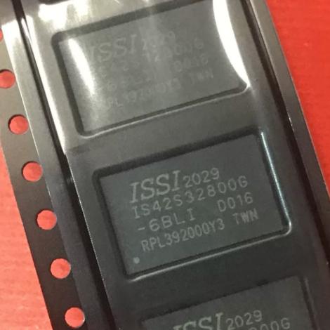
IS42S32800G-6BLI

128Mb SDR SDRAM, 4Mx32, 3.3V, 167MHz CL3, 4 banks, FBGA, industrial

1234

Effective Inventory

Image for reference only

Manufacturer Part:

IS42S32800G-6BLI

Package:

FBGA

Brand:

Product Categories:

Quality Commitment

Shipping & Payment

Service & Packaging

Product Manual

Description

Product Overview

The IS42S32800G-6BLI is a 128Mbit (4M x 8 x 4 banks) SDR SDRAM from ISSI organized as 4M x 32 with 3.3V supply and 167 MHz clock frequency (CL3). The x32 bus width makes it suitable for high-bandwidth embedded applications requiring wide data paths, such as DSP and FPGA external memory.

Key Specifications

Density 128Mbit
Standard SDR SDRAM
Organization 4M x 32
Supply Voltage 3.0V to 3.6V
Clock Frequency 167 MHz (CL3)
CAS Latency 2 or 3
Banks 4
Operating Temp -40°C to +85°C
Package FBGA
Part Status Active

Features

  • 128Mbit SDR SDRAM organized 4M x 32
  • 3.3V LVTTL interface
  • 167 MHz clock at CL=3
  • x32 wide data bus for high bandwidth
  • 4 internal banks for interleaved access
  • Programmable CAS latency (2 or 3)
  • Industrial temperature grade

Applications

  • DSP and FPGA external memory (x32 bus)
  • High-bandwidth video frame buffer
  • Networking ASIC wide-bus buffer
Product Introduction: IS42S32800G-6BLI Product Introduction

The IS42S32800G-6BLI is a 128Mbit SDR SDRAM from ISSI organized as 4M x 32 bits, operating at 3.3V with 167 MHz clock (CL3). The x32 wide data bus provides high bandwidth for DSP, FPGA, and video applications requiring wide memory paths. Four internal banks enable interleaved access for pipelined performance. Industrial temperature grade ensures reliable operation in harsh environments.

Working Principle: IS42S32800G-6BLI Working Principle

SDR SDRAM per JEDEC standard. The x32 organization provides 4x the bandwidth of x8 devices at the same clock frequency. Four internal banks with interleaved access hide precharge latency. Commands clocked on rising edge; single data rate transfer. Read: Activate + Read → data after CL cycles. Write: Activate + Write. Auto/self refresh maintains data integrity.

Pin Description: IS42S32800G-6BLI Pin Definition and Functions
Pin Group Interface Function
Address/Bank Input Address and bank select
DQ0-DQ31 I/O 32-bit data bus
DQM0-DQM3 Input Byte mask signals
CLK/CKE/CS#/Cmd Input Clock, enable, command
Application Scenarios: In which products and applications is IS42S32800G-6BLI used
  • FPGA external memory with 32-bit data path
  • DSP algorithm working memory
  • Video frame buffer with wide bus
Alternative Models: What chips are recommended as replacements for IS42S32800G-6BLI
Manufacturer Part Number Package Notes
ISSI IS42S16320F-6TLI TSOP 512Mbit x16 variant
Micron MT48LC4M32B2P-6A FBGA 128Mbit x32 SDRAM alternative

Recommend Parts

ISL95855HRTZ-T

IMVP8 3+2+1 phase buck controller, R3 technology, 4.5-25V input, 48-TQFN

Brand: Renesas

Package: 48-TQFN (6×6 mm, exposed pad)

IN STOCK: 2156pcs

Cargo cycle: 3-7 Days

The minimum order is 1

IRFB4019PBF

150V N-Channel HEXFET Power MOSFET, 47A, 34 mΩ RDS(on), TO-220AB

Brand: infineon

Package: TO-220AB

IN STOCK: 2409pcs

Cargo cycle: 3-7 Days

The minimum order is 1

MSP430F247TPMR

TI MSP430 MCU, 16-bit RISC, 92KB Flash, 8KB RAM, 16MHz, LQFP-64

Package: See datasheet

IN STOCK: 13371pcs

Cargo cycle: 3-7 Days

The minimum order is 1

UCC28740DR

CVCC Flyback Controller, 700V startup, opto feedback, <10mW no-load, SOIC-7

Brand: TI

Package: SOIC-7 (4.9 x 3.9 x 1.75 mm)

IN STOCK: 4840pcs

Cargo cycle: 3-7 Days

The minimum order is 1

MMUN2211LT1G

NPN digital transistor, R1=10kΩ R2=10kΩ, 50V, 100mA, SOT-23-3, pre-biased BRT switch

Brand: Onsemi

Package: SOT-23-3 (TO-236, SC-59)

IN STOCK: 8500pcs

Cargo cycle: 3-7 Days

The minimum order is 1

PIC32MX795F512L-80I/PF

32-bit PIC32MX MCU with Ethernet/CAN/USB, 80MHz, 512KB Flash, TQFP-100, industrial

Brand: MICROCHIP

Package: TQFP-100 (14 x 14 mm)

IN STOCK: 7912pcs

Cargo cycle: 3-7 Days

The minimum order is 1





