

Opens in a new tab

OP07CSZ

Ultralow offset voltage precision op-amp, 75µV VOS max, SOIC-8, ±3V to ±18V supply

6385

Effective Inventory

Image for reference only

Manufacturer Part:

OP07CSZ

Package:

SOIC-8 (4.9 x 3.9 mm)

Brand:

Quality Commitment

Shipping & Payment

Service & Packaging

Product Manual

Description

Product Overview

The OP07CSZ from Analog Devices is an ultralow offset voltage precision operational amplifier in an 8-lead SOIC package. With a maximum input offset voltage of 75µV (OP07E grade) and drift of 1.3µV/°C, it has become an industry standard for high-gain instrumentation applications. The device operates over a wide supply range of ±3V to ±18V and offers outstanding long-term stability of 1.5µV/month maximum.

Key Specifications

Supply Voltage Range ±3V to ±18V
Input Offset Voltage (OP07C) 60µV (typical), 150µV (max)
Offset Voltage Drift 1.3µV/°C (max, OP07E)
Input Bias Current 1.8nA (typical)
Open-Loop Gain 200V/mV (OP07E)
Gain Bandwidth Product 600kHz
Slew Rate 0.3V/µs
CMRR 106dB (OP07E), 120dB (typical)
Input Voltage Range ±14V (typical at ±15V supply)
Operating Temperature -40°C to +85°C
Package SOIC-8

Features

  • Ultralow VOS: 75µV maximum (OP07E grade)
  • Low offset drift: 1.3µV/°C maximum
  • Excellent long-term stability: 1.5µV/month maximum
  • Low noise: 0.6µV p-p maximum (0.1Hz to 10Hz)
  • Wide input voltage range: ±14V typical
  • High CMRR: 106dB (OP07E)
  • No external nulling required for most applications

Applications

  • Precision instrumentation amplifiers
  • Thermocouple and RTD signal conditioning
  • Strain gauge bridge amplifiers
  • Shunt current measurement
  • Precision active filters
  • Optical network control circuits
Product Introduction: OP07CSZ Product Introduction

The OP07CSZ is a precision operational amplifier from Analog Devices featuring ultralow input offset voltage achieved through wafer-level trimming. The OP07C grade specified over -40°C to +85°C offers typical offset voltage of 60µV and maximum CMRR of 120dB. The device eliminates the need for external nulling in most applications, simplifying circuit design. Its combination of low offset, low drift, high open-loop gain, and excellent CMRR makes it particularly suited for high-gain instrumentation where DC accuracy is critical. The wide ±3V to ±18V supply range and ±14V input voltage range provide flexibility in various signal conditioning applications.

Working Principle: OP07CSZ Working Principle

The OP07 employs a chopperless bipolar-input transistor amplifier circuit to achieve low offset and long-term stability without the switching noise associated with chopper-stabilized designs. Input offset voltage is trimmed at wafer level using electronically adjusted on-chip resistors (R2A/R2B), reducing VOS to 75µV maximum for the E grade. The bias-current cancellation circuitry provides low input bias current (±4nA for OP07E) while maintaining the low 1/f noise corner frequency characteristic. The true differential input with wide common-mode range and high CMRR (106dB OP07E) ensures maximum flexibility in noninverting configurations. The output stage drives loads directly without external buffering.

Pin Description: OP07CSZ Pin Definition and Functions
Pin Name Type Description
1 VOS TRIM Input Offset voltage trim terminal; connect to wiper of external nulling pot
2 -IN Input Inverting input
3 +IN Input Non-inverting input
4 V- Power Negative supply voltage
5 NC – No connect; leave floating or ground
6 OUT Output Amplifier output
7 V+ Power Positive supply voltage
8 VOS TRIM Input Offset voltage trim terminal; connect to other end of nulling pot
Application Scenarios: In which products and applications is OP07CSZ used
  • Thermocouple Signal Conditioning: Amplifies microvolt-level thermocouple outputs with minimal offset error, eliminating need for frequent recalibration in temperature measurement systems
  • Strain Gauge Bridge Amplifiers: Provides high-gain amplification of Wheatstone bridge outputs in load cells and pressure sensors with excellent DC accuracy
  • Shunt Current Measurement: Senses low-side current through shunt resistors with 120dB CMRR rejecting common-mode bus voltage variations
  • Precision Active Filters: Constructs low-frequency Sallen-Key or MFB filters where DC offset directly impacts filter accuracy
  • RTD Signal Conditioning: Amplifies PT100/PT1000 RTD signals with drift performance that maintains measurement accuracy over temperature
Alternative Models: What chips are recommended as replacements for OP07CSZ
Model Manufacturer VOS Max GBW Key Difference
OPA207AID TI 75µV 1.8MHz Lower power, wider bandwidth, improved drift
OPA202AID TI 75µV 1.8MHz Heavy capacitive load drive capability
OP07CPZ ADI 150µV 600kHz Same die in PDIP-8 package
OP27GSZ ADI 80µV 8MHz Much higher bandwidth, lower noise
ADA4077-1ARZ ADI 25µV 3.5MHz Newer precision amp with better all-around specs

Recommend Parts

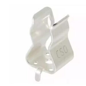
0751.0505

Schurter fuse, 0751.0505

Brand: schurter

Package: See datasheet

IN STOCK: 6768pcs

Cargo cycle: 3-7 Days

The minimum order is 1

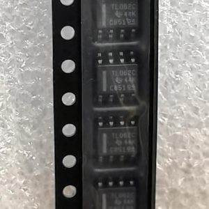
TL062CDR

Low-power JFET-input dual op-amp, 1MHz GBW, 30pA Ibias, SOIC-8, ±3.5V to ±18V

Brand: TI

Package: SOIC-8 (3.9 x 4.9 x 1.75mm)

IN STOCK: 11576pcs

Cargo cycle: 3-7 Days

The minimum order is 1

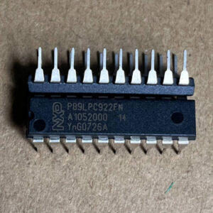
P89LPC922FN

8-bit 80C51 MCU, 8KB Flash, 256B RAM, 20-SSOP

Brand: NXP

Package: SSOP-20 (7.2 x 5.3 mm)

IN STOCK: 12628pcs

Cargo cycle: 3-7 Days

The minimum order is 1

AC0603JR-070RL

Chip Resistor, 0Ω (Zero Ohm Jumper), ±5%, 0603 (1608 Metric), 1/10W (100mW)

Brand: Yageo

Package: 0603 (1608 Metric)

IN STOCK: 100000pcs

Cargo cycle: 3-7 Days

The minimum order is 1

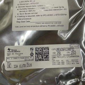
LMR34206FSC5RNXRQ1

42V 2A sync buck, 5V fixed, 2.2MHz, 18uA Iq, AEC-Q100, SOT-563

Brand: TI

Package: SOT-563 (1.6 x 1.2 x 0.55mm)

IN STOCK: 6500pcs

Cargo cycle: 3-7 Days

The minimum order is 1

AO3402

30V N-channel trench MOSFET, SOT-23, 4A, RDS(on) 52m ohm max @ 10V, Qg 10nC, 2.5V gate drive capable, -55C to +150C.

Brand: aosmd

Package: SOT-23 (2.9 x 1.6 x 1.25mm)

IN STOCK: 14066pcs

Cargo cycle: 3-7 Days

The minimum order is 1