
Opens in a new tab

SN74LS14N

Hex Schmitt-trigger inverter, 5V LS, 0.8V hysteresis, 22ns, PDIP-14

12000

Effective Inventory

Image for reference only

Manufacturer Part:

SN74LS14N

Package:

PDIP-14 (19.3 x 6.35 x 4.57mm, 2.54mm pitch, through-hole)

Brand:

Quality Commitment

Shipping & Payment

Service & Packaging

Product Manual

Description

Product Overview

The SN74LS14N is a hex Schmitt-trigger inverter from Texas Instruments with hysteresis inputs, high noise immunity, and slow-edge tolerance in a 14-pin PDIP package.

Key Specifications

Number of Channels 6 (hex inverter)
Logic Family LS (Low-power Schottky)
Supply Voltage 4.75V to 5.25V (5V nominal)
VT+ (Positive-going threshold) 1.5V min, 2.0V typical
VT- (Negative-going threshold) 0.6V typical, 1.0V max
Hysteresis (VT+ – VT-) 0.8V typical
Output Low Current (IOL) 8mA
Output High Current (IOH) -0.4mA
Propagation Delay 15ns typical, 22ns max at 5V
Supply Current 21mA max (all gates)
Input Type Schmitt-trigger with hysteresis
Output Type Push-pull (totem pole)
Operating Temperature 0°C to +70°C
Package PDIP-14 (19.3 x 6.35mm)

Features

  • Six independent Schmitt-trigger inverters in one package
  • Different threshold voltages for rising and falling inputs
  • High noise immunity due to hysteresis (~0.8V)
  • Operates from very slow input edges without oscillation
  • Improved line-receiving characteristics
  • Input clamp diodes limit negative undershoot
  • Direct replacement for 7414 and 74LS14 from any manufacturer
  • Temperature compensated thresholds

Applications

  • Switch debouncing and signal conditioning
  • Square wave generation from sine or triangle waves
  • RC oscillator circuits
  • Noisy signal cleanup and level restoration
  • Line receivers for long cable runs
Product Introduction: SN74LS14N Product Introduction

The SN74LS14N from Texas Instruments contains six independent Schmitt-trigger inverters in a 14-pin PDIP through-hole package. Unlike standard inverters that switch at a single threshold voltage, each Schmitt-trigger inverter has separate positive-going (VT+) and negative-going (VT-) thresholds with approximately 0.8V of hysteresis. This hysteresis provides high noise immunity and clean output switching even when the input signal has slow edges, noise, or bounce. The device converts slowly rising or falling analog signals into clean digital outputs without the oscillation that standard gates exhibit. The LS (Low-power Schottky) technology provides 15ns typical propagation delay with 8mA output sink current. Input clamp diodes protect against negative voltage undershoot. The N suffix denotes the PDIP through-hole package.

Working Principle: SN74LS14N Working Principle

Each of the six inverters in the SN74LS14N uses a Schmitt-trigger circuit with positive feedback that creates two distinct switching thresholds. When the input voltage rises from below VT- toward VT+, the output remains HIGH until the input exceeds VT+ (approximately 1.7V). Once the input crosses VT+, the output switches LOW. When the input then falls from above VT+ toward VT-, the output remains LOW until the input drops below VT- (approximately 0.9V). Only then does the output switch HIGH again. The difference between VT+ and VT- is the hysteresis voltage (approximately 0.8V), which creates a dead band where noise cannot cause the output to toggle. This is fundamentally different from a standard inverter (like the 74LS04) which switches at a single threshold around 1.3V and can oscillate if the input is near that threshold with noise. The Schmitt trigger’s hysteresis makes it ideal for switch debouncing: the bouncing contact creates a noisy input that oscillates between 0V and 5V, but the hysteresis ensures the output switches once and stays stable. The input clamp diode prevents the input from going below approximately -0.7V by clamping negative undershoot to ground.

Pin Description: SN74LS14N Pin Definition and Functions
Pin Name Type Description
1 1A Input Gate 1 input
2 1Y Output Gate 1 output
3 2A Input Gate 2 input
4 2Y Output Gate 2 output
5 3A Input Gate 3 input
6 3Y Output Gate 3 output
7 GND Power Ground
8 4Y Output Gate 4 output
9 4A Input Gate 4 input
10 5Y Output Gate 5 output
11 5A Input Gate 5 input
12 6Y Output Gate 6 output
13 6A Input Gate 6 input
14 VCC Power Supply (4.75V to 5.25V)

SN74LS14N uses the PDIP-14 package with the same hex inverter pinout as 7404/74LS04: VCC at Pin 14, GND at Pin 7. Six independent Schmitt-trigger inverters: Inv 1 (Pin 1 in, Pin 2 out), Inv 2 (Pin 3 in, Pin 4 out), Inv 3 (Pin 5 in, Pin 6 out), Inv 4 (Pin 9 in, Pin 8 out), Inv 5 (Pin 11 in, Pin 10 out), Inv 6 (Pin 13 in, Pin 12 out). The Schmitt-trigger inputs have hysteresis of approximately 0.8V (VT+ ≈ 1.7V, VT- ≈ 0.9V) at 5V supply. This makes the device ideal for cleaning up noisy signals, debouncing mechanical switches, and building RC oscillators. For wider supply range, 74HC14 operates from 2-6V with proportional hysteresis.

Application Scenarios: In which products and applications is SN74LS14N used
  • Switch Debouncing: 0.8V hysteresis eliminates contact bounce without software delays; output is clean single-edge
  • Signal Squaring: Converts slow sine, triangle, or ramp signals into clean digital square waves without multi-transition
  • RC Oscillator: One gate plus one resistor and one capacitor form a simple square-wave oscillator; hysteresis sets frequency
  • Noise Cleanup: Restores degraded digital signals from long cables; hysteresis rejects noise within the dead band
  • Line Receiver: Improved line-receiving characteristics over standard gates for noisy TTL signal reception
Alternative Models: What chips are recommended as replacements for SN74LS14N
Model Manufacturer Key Difference Package Supply
74LS14N TI/Nexperia Original TTL version with 5V-only supply, typical propagation delay 10-15ns DIP-14 5V TTL
74LS14D TI/Nexperia Surface-mount SOIC version of LS with identical logic function SOIC-14 5V TTL
74HC14D TI/Nexperia CMOS version with wide 2-6V supply range, lower power consumption and higher noise immunity SOIC-14 2-6V CMOS
74HC14N TI/Nexperia Through-hole DIP version of HC family for prototyping and repair DIP-14 2-6V CMOS
74HCT14D TI/Nexperia CMOS with TTL-compatible input levels, ideal for mixing with LS devices at 5V SOIC-14 4.5-5.5V TTL-in
74HCT14N TI/Nexperia Through-hole DIP version of HCT family for prototyping and repair DIP-14 4.5-5.5V TTL-in
74AC14D TI/Nexperia Advanced CMOS with 2-6V supply and higher output drive current (24mA vs 6mA for HC) SOIC-14 2-6V CMOS
74AC14N TI/Nexperia Through-hole DIP version of AC family for prototyping and repair DIP-14 2-6V CMOS
74LVC14D TI/Nexperia Low-voltage CMOS for 1.65-3.6V modern logic with 24mA output drive and bus-hold inputs SOIC-14 1.65-3.6V CMOS
74LVC14N TI/Nexperia Through-hole DIP version of LVC family for prototyping and repair DIP-14 1.65-3.6V CMOS

The 7414 is a Hex Schmitt-Trigger Inverter. Family variants span from the original LS TTL (5V only) to modern LVC/AUP (down to 0.8V). HC and HCT versions offer 2-6V CMOS operation with HCT providing TTL-compatible input thresholds for mixed 5V systems. CD4000-series equivalents offer the widest 3-18V supply range at the cost of lower switching speed. DIP packages (N suffix) are through-hole; SOIC (D suffix) and TSSOP are surface-mount.

Recommend Parts

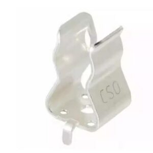
0751.0505

Schurter fuse, 0751.0505

Brand: schurter

Package: See datasheet

IN STOCK: 6768pcs

Cargo cycle: 3-7 Days

The minimum order is 1

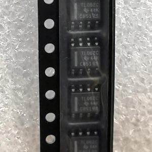
TL062CDR

Low-power JFET-input dual op-amp, 1MHz GBW, 30pA Ibias, SOIC-8, ±3.5V to ±18V

Brand: TI

Package: SOIC-8 (3.9 x 4.9 x 1.75mm)

IN STOCK: 11576pcs

Cargo cycle: 3-7 Days

The minimum order is 1

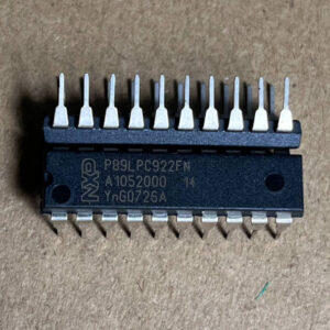
P89LPC922FN

8-bit 80C51 MCU, 8KB Flash, 256B RAM, 20-SSOP

Brand: NXP

Package: SSOP-20 (7.2 x 5.3 mm)

IN STOCK: 12628pcs

Cargo cycle: 3-7 Days

The minimum order is 1

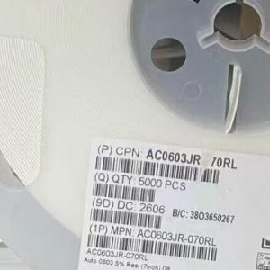
AC0603JR-070RL

Chip Resistor, 0Ω (Zero Ohm Jumper), ±5%, 0603 (1608 Metric), 1/10W (100mW)

Brand: Yageo

Package: 0603 (1608 Metric)

IN STOCK: 100000pcs

Cargo cycle: 3-7 Days

The minimum order is 1

LMR34206FSC5RNXRQ1

42V 2A sync buck, 5V fixed, 2.2MHz, 18uA Iq, AEC-Q100, SOT-563

Brand: TI

Package: SOT-563 (1.6 x 1.2 x 0.55mm)

IN STOCK: 6500pcs

Cargo cycle: 3-7 Days

The minimum order is 1

AO3402

30V N-channel trench MOSFET, SOT-23, 4A, RDS(on) 52m ohm max @ 10V, Qg 10nC, 2.5V gate drive capable, -55C to +150C.

Brand: aosmd

Package: SOT-23 (2.9 x 1.6 x 1.25mm)

IN STOCK: 14066pcs

Cargo cycle: 3-7 Days

The minimum order is 1