






Opens in a new tab

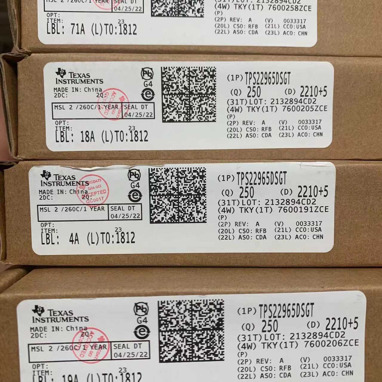
TPS22965DSGT

Single-channel load switch, 0.8-5.7V input, 6A max current, 16mΩ RON, configurable rise time, WSON-8

9847

Effective Inventory

Image for reference only

Manufacturer Part:

TPS22965DSGT

Package:

WSON-8 (DSG) – 2.0 x 2.0 x 0.8 mm, 0.5mm pitch

Brand:

Quality Commitment

Shipping & Payment

Service & Packaging

Product Manual

Description

Product Overview

The TPS22965DSGT is a single-channel load switch from Texas Instruments featuring ultra-low on-resistance and configurable rise time for inrush current control. The device integrates an N-channel MOSFET that operates over an input voltage range of 0.8 V to 5.7 V and supports a maximum continuous current of 6 A. With an on-resistance of just 16 mΩ at 5 V input, this load switch minimizes voltage drop and power loss in high-current power rails.

Packaged in an 8-pin WSON (DSG) package measuring 2.0 mm × 2.0 mm with an exposed thermal pad, the TPS22965 provides excellent thermal performance for its size. The CT pin allows the user to program the output rise time via an external capacitor, enabling precise control of inrush current when driving capacitive loads. A quick output discharge (QOD) feature connects a 225 Ω resistor between VOUT and GND when the switch is disabled, preventing the output from floating.

The device operates over the temperature range of –40°C to +105°C and features very low leakage current during the off state, making it ideal for battery-powered systems where standby power consumption is critical. The low-voltage control input threshold allows direct interfacing with 1.2 V, 1.8 V, 2.5 V, and 3.3 V logic levels.

Key Specifications

Parameter Value
Input Voltage Range 0.8 V to 5.7 V
Bias Voltage Range 2.5 V to 5.7 V
Maximum Continuous Current 6 A
On-Resistance (RON) 16 mΩ typical @ VIN = 5 V (VBIAS = 5 V)
On-Resistance 16 mΩ typical @ VIN = 3.6 V (VBIAS = 5 V)
Quiescent Current 50 µA typical
Off-State Leakage 0.01 µA typical @ VIN = 1.8 V
Rise Time Control Configurable via CT capacitor
Quick Output Discharge 225 Ω on-chip resistor
Logic Threshold Compatible with 1.2V, 1.8V, 2.5V, 3.3V logic
Package WSON-8 (DSG), 2.0 x 2.0 mm
Operating Temperature –40°C to +105°C

Features

  • Integrated single-channel load switch with ultra-low RON (16 mΩ)
  • Wide input voltage range: 0.8 V to 5.7 V
  • High current capability: 6 A continuous, 8 A pulsed
  • Configurable rise time via CT pin capacitor for inrush control
  • Quick output discharge (QOD) with 225 Ω on-chip resistor
  • Very low off-state leakage current (0.01 µA typical)
  • Low control input threshold supports 1.2V, 1.8V, 2.5V, 3.3V logic
  • Foldback overcurrent protection
  • 8-pin WSON package with exposed thermal pad
  • ESD performance: 2000 V HBM, 1000 V CDM per JESD 22
  • RoHS compliant, green packaging

Applications

  • Ultrabooks, notebooks, and netbooks
  • Tablet PCs and portable electronics
  • Solid-state drives (SSDs) and storage systems
  • Consumer electronics and set-top boxes
  • Residential gateways and telecom systems
  • Battery-powered devices with power gating
  • Dynamic power domain switching for low-power modes
  • Peripheral power management in handheld devices

Product Introduction: TPS22965DSGT Product Introduction

The TPS22965DSGT is a high-performance single-channel load switch from Texas Instruments, designed for power distribution and power domain management in portable and consumer electronics. Featuring an ultra-low on-resistance of 16 mΩ across a wide input voltage range, this device efficiently handles up to 6 A of continuous current while minimizing power loss and voltage drop across the switch.

At the heart of the TPS22965 is an N-channel MOSFET with a dedicated charge pump driver that provides full gate enhancement for low RON operation. The VBIAS pin supplies the internal control circuitry and charge pump, allowing the main power path (VIN to VOUT) to operate at voltages as low as 0.8 V. This dual-supply architecture is particularly useful in systems where a low-voltage rail must be switched but a higher voltage bias supply is available.

A key feature of the TPS22965 is its configurable rise time, controlled by an external capacitor on the CT pin. This allows designers to precisely tailor the output slew rate to match the load capacitance, minimizing inrush current and preventing supply voltage droop during turn-on. The quick output discharge feature provides a controlled discharge path when the switch is disabled, ensuring that downstream circuitry fully powers down and preventing floating node issues.

Available in a compact 8-pin WSON package with exposed thermal pad, the TPS22965DSGT offers excellent thermal performance in a minimal board footprint. The device operates over the full industrial temperature range of -40°C to +105°C and is fully RoHS compliant.

Working Principle: TPS22965DSGT Working Principle

The TPS22965 load switch operates using several key functional blocks:

1. N-Channel Power MOSFET: The main power path consists of an N-channel MOSFET that connects VIN to VOUT when enabled. N-channel devices are used for their lower RON per area compared to P-channel devices, but require a gate drive voltage higher than the input voltage.

2. Charge Pump / Gate Driver: An integrated charge pump generates a voltage above VBIAS to fully enhance the gate of the N-channel MOSFET, achieving the minimum RON. This ensures low voltage drop even at full load current.

3. Rise Time Control (CT Pin): The CT pin controls the slew rate of the output voltage. An external capacitor connected from CT to GND sets the rate at which the gate is charged, directly controlling the output rise time. The relationship is approximately: SR = 0.38 × CT + 34 (µs/V). This is critical for limiting inrush current into capacitive loads.

4. Quick Output Discharge (QOD): When the switch is disabled (ON pin low), an internal 225 Ω resistor is connected between VOUT and GND. This actively discharges the output capacitor, preventing the output from floating and ensuring a known state for downstream circuits.

5. Control Logic: The ON pin provides enable/disable control. The input threshold is designed to be compatible with low-voltage logic (1.2 V to 3.3 V), allowing direct interface with microcontroller I/Os without level shifting.

6. Protection Features: The device includes undervoltage lockout (UVLO) on VBIAS, over-temperature protection, and overcurrent protection to ensure robust operation under fault conditions.

Pin Description: TPS22965DSGT Pin Definition and Functions
Pin No. Pin Name Type Function
1 VOUT Output Load switch output. Connect to load circuitry.
2 VOUT Output Load switch output (bonded together internally with pin 1).
3 GND Ground Ground reference for all internal circuitry.
4 ON Input Enable input. Drive high to turn on the switch. Compatible with 1.2V/1.8V/2.5V/3.3V logic.
5 CT Input Slew rate control pin. Connect a capacitor to GND to set output rise time. Leave open for fastest rise time.
6 VBIAS Power Bias supply voltage for internal control circuitry and charge pump. Range: 2.5V to 5.7V. Bypass with 1uF ceramic capacitor.
7 VIN Input Load switch input. Connect to input power supply. Range: 0.8V to VBIAS.
8 VIN Input Load switch input (bonded together internally with pin 7).
Pad Thermal Pad Ground Exposed thermal pad. Must be soldered to PCB ground for proper thermal dissipation.

Note: Pins 1/2 and pins 7/8 are internally bonded together for improved current handling and thermal performance. Both pins should be connected on the PCB for optimal performance.

Application Scenarios: In which products and applications is TPS22965DSGT used
  • Notebook and Tablet Power Management: Power gating for peripheral subsystems (display, audio, sensors) to reduce standby power consumption and extend battery life. The low off-state leakage is critical in always-on systems.
  • Solid-State Drives (SSDs): Switching power rails for NAND flash arrays and controller cores. The 6A current capability supports high-density SSD designs with multiple flash channels.
  • Consumer Electronics: Set-top boxes, residential gateways, and telecom equipment where dynamic power domain switching is used for power management and fault isolation.
  • Battery-Powered Devices: Wearables, IoT sensors, and handheld instruments where sub-circuits are powered down to minimize drain on the battery during idle periods.
  • Hot-Plug and Hot-Swap Applications: Controlling power to removable modules or peripherals, with controlled slew rate to prevent back-powering and minimize disturbance to the main supply.
  • FPGA and ASIC Power Sequencing: Providing power-up sequencing between different voltage domains in multi-rail systems, where load switches offer a simpler alternative to complex power ICs for sequencing.
Alternative Models: What chips are recommended as replacements for TPS22965DSGT
Manufacturer Part Number Vin (V) Iout (A) Notes
Texas Instruments TPS22966DSGR 0.8-5.7 4 4A version, same package
Texas Instruments TPS22965NDSGT 0.8-5.7 6 No QOD, same pinout
Texas Instruments TPS22964DSGR 0.8-5.7 2 2A version, smaller package option
Diodes Inc. AP2551AW6-7 2.5-5.5 6 Alternative 6A load switch
ON Semiconductor NCP45520IMNTWG 1.5-5.5 2 Low-cost 2A alternative
Vishay SiP4280DY-T1-E3 1.6-5.5 3 3A load switch with fault flag

Recommend Parts

ISO1176TDWR

Isolated RS-485 transceiver, 40Mbps, integrated transformer driver, SOIC-16

Brand: TI

Package: SOIC-16 (DW, wide-body, 10.3 x 10.3 mm)

IN STOCK: 6874pcs

Cargo cycle: 3-7 Days

The minimum order is 1

IRFB4020PBF

200V N-Channel HEXFET Power MOSFET, 31A, 68 mΩ RDS(on), TO-220AB

Brand: infineon

Package: TO-220AB

IN STOCK: 14149pcs

Cargo cycle: 3-7 Days

The minimum order is 1

NRF52832-QFAA-T

Nordic BLE SoC, ARM Cortex-M4 @ 64MHz, 64KB Flash, 32KB RAM, QFN-48

Package: See datasheet

IN STOCK: 10958pcs

Cargo cycle: 3-7 Days

The minimum order is 1

UCC28740DR

CVCC Flyback Controller, 700V startup, opto feedback, <10mW no-load, SOIC-7

Brand: TI

Package: SOIC-7 (4.9 x 3.9 x 1.75 mm)

IN STOCK: 4840pcs

Cargo cycle: 3-7 Days

The minimum order is 1

MMUN2211LT1G

NPN digital transistor, R1=10kΩ R2=10kΩ, 50V, 100mA, SOT-23-3, pre-biased BRT switch

Brand: Onsemi

Package: SOT-23-3 (TO-236, SC-59)

IN STOCK: 8500pcs

Cargo cycle: 3-7 Days

The minimum order is 1

TMS320F2810PBKA

C2000 Delfino DSP controller, 150MHz, 128KB Flash, BGA-179

Brand: TI

Package: BGA-179 (16 x 16 mm, PBK package)

IN STOCK: 3124pcs

Cargo cycle: 3-7 Days

The minimum order is 1




