






Opens in a new tab

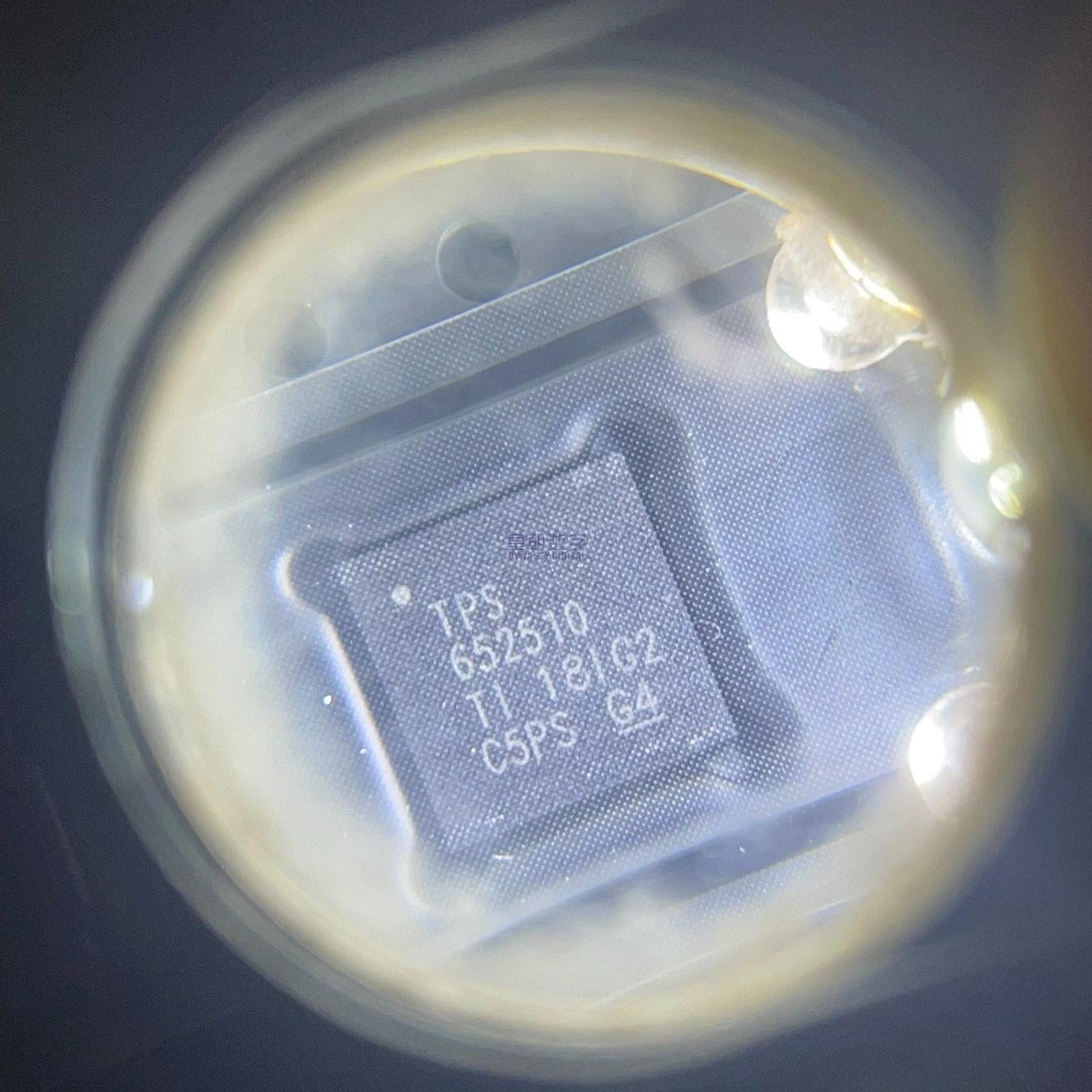
TPS65250RHAR

Triple synchronous buck converter, 4.5-18V input, 3A+2A+2A output, 1.5MHz, VQFN-40, industrial multi-rail PSU

6289

Effective Inventory

Image for reference only

Manufacturer Part:

TPS65250RHAR

Package:

VQFN-40 (RHA) – 6.0 x 6.0 x 1.0 mm, 0.5mm pitch

Brand:

Quality Commitment

Shipping & Payment

Service & Packaging

Product Manual

Description

Product Overview

The TPS65250RHAR is a triple synchronous step-down DC/DC converter from Texas Instruments, designed for applications requiring multiple high-efficiency low-voltage power rails. The device integrates three independent synchronous buck converters that operate at 1.5 MHz fixed frequency and can deliver up to 3 A, 2 A, and 2 A of output current respectively.

Packaged in a 40-pin VQFN (RHA) package measuring 6 mm × 6 mm with 0.5 mm pitch, the TPS65250 operates from a single 4.5 V to 18 V input supply. Each converter has a dedicated enable input, power-good output, and adjustable soft-start. The converters operate 180° out-of-phase (Buck2 and Buck3 shifted relative to Buck1), reducing input ripple current and EMI.

All three converters feature integrated high-side and low-side MOSFETs, current-mode control, cycle-by-cycle current limit, thermal shutdown, and output overvoltage protection. The device also includes two low-side driver outputs that can be used to drive an external N-channel MOSFET for inrush current limiting or load switching. With an operating temperature range of –40°C to +85°C, the TPS65250RHAR is well-suited for industrial, communications, and consumer multi-rail power systems.

Key Specifications

Parameter Buck1 Buck2 Buck3
Input Voltage 4.5 V to 18 V (single input)
Output Voltage Range 0.765 V to 7 V (adjustable)
Output Current 3 A 2 A 2 A
Switching Frequency 1.5 MHz fixed (synchronized, 180° phase shift)
Top FET RON 90 mΩ 120 mΩ 120 mΩ
Bottom FET RON 60 mΩ 80 mΩ 80 mΩ
Reference Voltage 0.765 V (±1.5% accuracy)
Quiescent Current (per buck) 70 µA typical
Shutdown Current 10 µA typical (all bucks disabled)
Package VQFN-40 (RHA), 6 x 6 mm
Operating Temperature –40°C to +85°C

Features

  • Three independent synchronous step-down converters in a single package
  • Wide input voltage range: 4.5 V to 18 V (supports 5V, 12V, and battery inputs)
  • Output currents: Buck1: 3 A, Buck2: 2 A, Buck3: 2 A
  • Adjustable output voltage: 0.765 V to 7 V per channel
  • Fixed 1.5 MHz switching frequency with out-of-phase operation
  • Integrated high-side and low-side power MOSFETs
  • Peak current-mode control for fast transient response
  • Internal soft-start with adjustable time via external capacitor
  • Individual enable inputs and power-good outputs per channel
  • Cycle-by-cycle current limit and hiccup-mode short-circuit protection
  • Output overvoltage and undervoltage protection
  • Thermal shutdown protection with hysteresis
  • Two integrated low-side gate drivers for external N-channel FETs
  • 40-pin VQFN package (6 mm × 6 mm) with exposed thermal pad

Applications

  • Industrial control and automation systems
  • Telecommunications and networking equipment
  • Set-top boxes and residential gateways
  • Consumer electronics and home appliances
  • Server and storage systems
  • Point-of-load (POL) power supplies
  • Multi-rail FPGA and DSP power solutions
  • Test and measurement equipment
Product Introduction: TPS65250RHAR Product Introduction

The TPS65250RHAR is a highly integrated triple-channel synchronous step-down DC/DC converter from Texas Instruments. Designed for applications requiring multiple regulated low-voltage rails from a higher-voltage input, this device combines three independent buck converters into a single 40-pin VQFN package, significantly reducing component count, PCB area, and system cost compared to discrete solutions.

Operating from a wide 4.5 V to 18 V input range, the TPS65250 can be powered from 5V, 12V, or multi-cell battery supplies. Buck1 provides up to 3 A of output current, while Buck2 and Buck3 each deliver up to 2 A. Each converter has an adjustable output voltage range of 0.765 V to 7 V, set via an external resistor divider from the 0.765 V internal reference.

All three converters operate at a fixed 1.5 MHz switching frequency using peak current-mode control, providing excellent line and load transient response. The converters operate with 180° phase shift between channels (Buck2 and Buck3 are 180° out of phase with Buck1), which reduces input ripple current and the required input capacitance, lowering both cost and EMI.

Each channel has dedicated enable and power-good pins, allowing independent control and monitoring. Integrated soft-start circuitry, with adjustable timing via external capacitors, ensures controlled inrush current during startup. The device includes comprehensive protection features: cycle-by-cycle current limit, hiccup-mode short circuit protection, output overvoltage protection, undervoltage lockout, and thermal shutdown.

Additionally, the TPS65250 includes two low-side gate driver outputs (LDO1 and LDO2 pins) capable of driving external N-channel MOSFETs for load switch or inrush control applications.

Working Principle: TPS65250RHAR Working Principle

The TPS65250 contains three independent synchronous buck converters with the following operating principles:

1. Control Architecture: Each converter uses fixed-frequency peak current-mode control. The inner current loop regulates peak inductor current by comparing the current sense signal to the error amplifier output. The outer voltage loop regulates the output voltage through the error amplifier, which compares the feedback voltage to the internal 0.765 V bandgap reference.

2. Synchronous Rectification: Each converter integrates both a high-side (control) and low-side (synchronous) N-channel MOSFET. The low-side FET conducts during the off-time of the high-side FET, providing a low-loss current path that significantly improves efficiency compared to diode rectification, especially at low output voltages.

3. Out-of-Phase Operation: Buck2 and Buck3 operate 180° out of phase with Buck1. This interleaving reduces the peak input current drawn from the supply, reducing input ripple and allowing the use of smaller input capacitors. It also reduces conducted and radiated EMI.

4. Soft-Start: Each channel has an internal soft-start circuit that ramps the reference voltage during startup. An external capacitor on the SS pin can be used to extend the soft-start time, reducing inrush current when driving large capacitive loads.

5. Current Limit and Protection: Cycle-by-cycle peak current limit protects the power MOSFETs and inductor from overcurrent conditions. If the output is shorted, the device enters hiccup mode, periodically retrying to limit power dissipation. Output overvoltage protection clamps the output if it exceeds regulation limits.

6. Low-Side Drivers: Two integrated low-side drivers (LSD1 and LSD2) can drive external N-channel MOSFETs for use as load switches or inrush current limiters. These are controlled via the EN_LSD pins.

Pin Description: TPS65250RHAR Pin Definition and Functions
Pin No. Pin Name Type Function
1-2 VIN1 Power Buck1 input supply. Bypass with ceramic capacitor to PGND1.
3 EN1 Input Buck1 enable input. High = enabled, low = disabled.
4 PGOOD1 Output Buck1 power-good output (open drain, requires pull-up resistor).
5 SS1 Input Buck1 soft-start. Connect capacitor to GND to set soft-start time.
6 FB1 Input Buck1 feedback input. Connect to output voltage divider.
7 SW1 Output Buck1 switch node. Connect to inductor and bootstrap capacitor.
8 BOOT1 Input Buck1 bootstrap supply. Connect 100nF cap between BOOT1 and SW1.
9 PGND1 Ground Buck1 power ground
10-11 VIN2 Power Buck2 input supply
12 EN2 Input Buck2 enable input
13 PGOOD2 Output Buck2 power-good output
14 SS2 Input Buck2 soft-start
15 FB2 Input Buck2 feedback input
16 SW2 Output Buck2 switch node
17 BOOT2 Input Buck2 bootstrap supply
18 PGND2 Ground Buck2 power ground
19 AGND Ground Analog ground (reference for all control circuits)
20 V5 Output Internal 5V regulator output. Bypass with 2.2uF ceramic to AGND.
21 LSD2 Output Low-side driver 2 output for external N-channel MOSFET
22 EN_LSD2 Input Low-side driver 2 enable input
23 LSD1 Output Low-side driver 1 output for external N-channel MOSFET
24 EN_LSD1 Input Low-side driver 1 enable input
25 VIN_LSD Power Low-side drivers supply voltage
26-27 VIN3 Power Buck3 input supply
28 EN3 Input Buck3 enable input
29 PGOOD3 Output Buck3 power-good output
30 SS3 Input Buck3 soft-start
31 FB3 Input Buck3 feedback input
32 SW3 Output Buck3 switch node
33 BOOT3 Input Buck3 bootstrap supply
34 PGND3 Ground Buck3 power ground
35-40 EP Ground Exposed thermal pad. Must connect to ground plane.

Note: Full pin details and recommended layout are available in the datasheet. The exposed thermal pad should be connected to the ground plane with multiple vias for optimal thermal performance.

Application Scenarios: In which products and applications is TPS65250RHAR used
  • Industrial Control Systems: Powering multiple voltage rails in PLC modules, motor drives, and factory automation equipment where 12V or 24V input is stepped down to 5V, 3.3V, and 1.8V.
  • Telecommunications and Networking: Multi-rail power supplies for routers, switches, and telecom modules, providing core, I/O, and memory voltages from a 12V system bus.
  • FPGA and DSP Power: Power supply solutions for FPGA, DSP, and ASIC designs requiring multiple tightly-regulated voltage rails with sequencing and power-good signaling.
  • Set-Top Boxes and Gateways: Consumer electronics and residential gateway devices needing multiple efficient DC-DC converters from a 12V adapter supply.
  • Server and Storage Systems: Point-of-load (POL) converters in server motherboards and storage arrays, providing secondary regulation from a 12V intermediate bus.
  • Test and Measurement Equipment: Benchtop and portable instruments requiring multiple high-efficiency power rails with good regulation and transient response.
  • Automotive Infotainment: Infotainment and ADAS systems (with appropriate front-end protection) where the 12V battery supply must generate several low-voltage rails for processors, memories, and peripherals.
Alternative Models: What chips are recommended as replacements for TPS65250RHAR
Manufacturer Part Number Vin (V) Channels Notes
Texas Instruments TPS65251RHAR 4.5-18 4 (3A+2A+2A+2A) Fourth buck converter added
Texas Instruments TPS54302DDCR 4.5-18 1 (3A) Single 3A buck, SOT-23
Texas Instruments LM26420YMH 2.8-5.5 2 (2A+2A) Dual buck, lower voltage input
Analog Devices LTM4638MPY 3.6-15 3 (3A+2A+2A) µModule alternative, more integrated
MPS MPM8626QGVE 4.5-16 2 (6A+6A) Module, higher current
Infineon IR38060MTRPBF 5-21 1 (6A) High-current single buck, SupIRBuck

Recommend Parts

ISO1176TDWR

Isolated RS-485 transceiver, 40Mbps, integrated transformer driver, SOIC-16

Brand: TI

Package: SOIC-16 (DW, wide-body, 10.3 x 10.3 mm)

IN STOCK: 6874pcs

Cargo cycle: 3-7 Days

The minimum order is 1

IRFB4020PBF

200V N-Channel HEXFET Power MOSFET, 31A, 68 mΩ RDS(on), TO-220AB

Brand: infineon

Package: TO-220AB

IN STOCK: 14149pcs

Cargo cycle: 3-7 Days

The minimum order is 1

NRF52832-QFAA-T

Nordic BLE SoC, ARM Cortex-M4 @ 64MHz, 64KB Flash, 32KB RAM, QFN-48

Package: See datasheet

IN STOCK: 10958pcs

Cargo cycle: 3-7 Days

The minimum order is 1

UCC28740DR

CVCC Flyback Controller, 700V startup, opto feedback, <10mW no-load, SOIC-7

Brand: TI

Package: SOIC-7 (4.9 x 3.9 x 1.75 mm)

IN STOCK: 4840pcs

Cargo cycle: 3-7 Days

The minimum order is 1

MMUN2211LT1G

NPN digital transistor, R1=10kΩ R2=10kΩ, 50V, 100mA, SOT-23-3, pre-biased BRT switch

Brand: Onsemi

Package: SOT-23-3 (TO-236, SC-59)

IN STOCK: 8500pcs

Cargo cycle: 3-7 Days

The minimum order is 1

TMS320F2810PBKA

C2000 Delfino DSP controller, 150MHz, 128KB Flash, BGA-179

Brand: TI

Package: BGA-179 (16 x 16 mm, PBK package)

IN STOCK: 3124pcs

Cargo cycle: 3-7 Days

The minimum order is 1





