
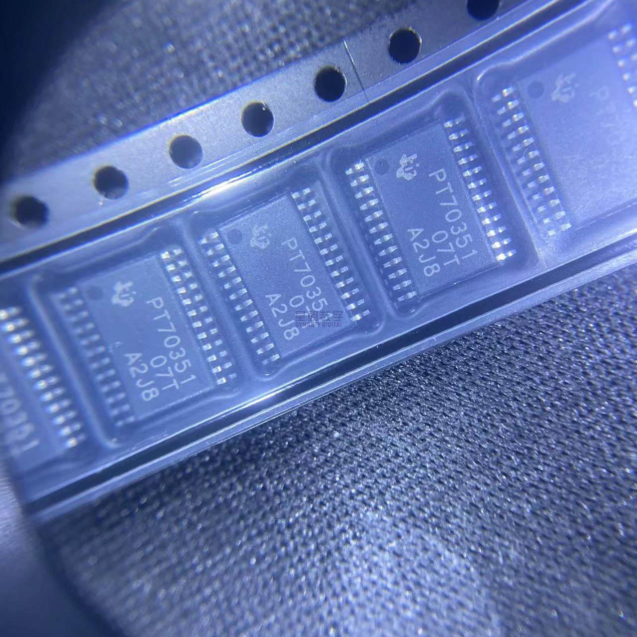






Opens in a new tab

TPS70351PWPR

Dual LDO regulator + supervisor, 3.3V+1.8V/2.5V at 1A each, power sequencing, reset+power-good, HTSSOP-24

7345

Effective Inventory

Image for reference only

Manufacturer Part:

TPS70351PWPR

Package:

HTSSOP-24 (PWP) – 7.8 x 4.4 x 1.2 mm, 0.65mm pitch, PowerPAD

Brand:

Quality Commitment

Shipping & Payment

Service & Packaging

Product Manual

Description

Product Overview

The TPS70351PWPR is a dual-channel low-dropout (LDO) voltage regulator with integrated supervisory circuits from Texas Instruments, designed specifically to power TI TMS320 DSPs and other multi-rail embedded processors. The device provides two independently controlled LDO outputs and includes a power-on reset supervisor, undervoltage monitoring, and manual reset input for complete power management and system reset control in a single package.

Packaged in a 24-pin HTSSOP (PWP) package measuring 7.8 mm × 4.4 mm with 0.65 mm pitch, the TPS70351 operates from a single 3 V to 5.5 V input supply. The dual regulators produce fixed output voltages of 3.3 V (Reg1) and 1.8 V / 2.5 V (Reg2, selectable), each with a maximum output current of 1 A. The device features a sequential power-up capability where Reg2 turns on after Reg1 reaches regulation, satisfying the power-up sequencing requirements of many DSP and processor cores.

Integrated supervisory features include a power-on reset (RESET) output with programmable delay, a manual reset input (/MR), an open-drain power-good output, and undervoltage sensing on both outputs. The device also offers a thermal shutdown protection circuit and reverse battery protection. Operating over the temperature range of –40°C to +125°C, the TPS70351PWPR is suitable for industrial, communications, and computing applications requiring a compact, integrated power solution.

Key Specifications

Parameter Regulator 1 Regulator 2
Input Voltage Range 3.0 V to 5.5 V (single supply)
Output Voltage 3.3 V (fixed) 1.8 V / 2.5 V (selectable via SEL pin)
Output Current 1 A 1 A
Dropout Voltage 220 mV @ 1 A 200 mV @ 1 A
Output Accuracy ±2% (over temperature)
Quiescent Current 1.5 mA typical (both enabled)
PSRR 60 dB typical @ 1 kHz
Enable/Sequence Independent EN1 EN2 + auto-sequencing option
Supervisor Features Power-on reset, manual reset, power-good, UV monitor
Package HTSSOP-24 (PWP), 7.8 x 4.4 mm
Operating Temperature –40°C to +125°C

Features

  • Dual LDO regulators: 3.3 V/1 A + 1.8 V or 2.5 V/1 A
  • Low dropout: 220 mV at 1 A (Reg1), 200 mV at 1 A (Reg2)
  • Single input supply: 3.0 V to 5.5 V
  • Selectable Reg2 output (1.8 V or 2.5 V) via SEL pin
  • Programmable power-up sequencing (Reg1 then Reg2)
  • Power-on reset (RESET) output with 200 ms delay Manual reset input (/MR) with debounce
  • Open-drain power-good (PG) output Undervoltage monitoring on both outputs
  • Thermal shutdown and overcurrent protection
  • Reverse battery protection on VIN
  • High PSRR: 60 dB at 1 kHz
  • 24-pin HTSSOP package with PowerPAD™ thermal pad
  • Industrial temperature range: –40°C to +125°C
  • Pin-compatible with TPS703xx family

Applications

  • Power supply for DSP, MCU, and FPGA systems
  • TI TMS320C6000 and OMAP processor power
  • Industrial control and automation equipment
  • Telecommunications and networking hardware
  • Embedded systems and single-board computers
  • Test and measurement instruments
  • Medical and healthcare equipment
  • Multi-rail supplies requiring power sequencing

Product Introduction: TPS70351PWPR Product Introduction

The TPS70351PWPR is a highly integrated dual-channel low-dropout regulator with comprehensive supervisory features from Texas Instruments. Designed specifically to power TI TMS320 DSPs and other multi-rail microprocessors, this device combines two high-current LDO regulators with power-on reset, manual reset, power-good monitoring, and power sequencing control in a single 24-pin HTSSOP package.

Regulator 1 provides a fixed 3.3V output at up to 1A, typically used for I/O and peripheral power. Regulator 2 provides a selectable 1.8V or 2.5V output at up to 1A, suitable for DSP core or memory supply voltages. The output voltage of Regulator 2 is selected via the SEL pin, which can be tied high for 2.5V or low for 1.8V, providing flexibility for different system requirements.

A key feature of the TPS70351 is its programmable power sequencing capability. The device can be configured so that Regulator 2 automatically turns on after Regulator 1 reaches regulation and a programmed delay has elapsed. This ensures compliance with the specific power-up sequencing requirements of DSPs, FPGAs, and other sensitive digital ICs, preventing latch-up and ensuring reliable system initialization.

The integrated supervisory circuitry includes a power-on reset (POR) generator that asserts the RESET output during power-up and maintains it for a fixed delay (typically 200ms) after both regulators have reached regulation. A manual reset input allows external reset sources to trigger a system reset, while the power-good output provides a signal indicating that all outputs are within their specified voltage ranges. Undervoltage detection on both regulators provides early warning of impending power failure.

Using TI’s PowerPAD package technology for enhanced thermal performance, the TPS70351PWPR operates over the full industrial temperature range of -40°C to +125°C and is fully specified for operation across this range.

Working Principle: TPS70351PWPR Working Principle

The TPS70351 integrates two independent LDO regulators and supervisory circuitry:

1. LDO Regulator Architecture: Each regulator uses a P-channel pass transistor in a classic LDO topology. A bandgap reference voltage provides a temperature-stable reference to an error amplifier, which compares a fraction of the output voltage (from an internal resistor divider) against the reference and adjusts the gate of the PMOS pass element to maintain regulation. The P-channel architecture allows low dropout voltage and operation from a low input supply.

2. Power Sequencing: When configured for sequential operation, Regulator 2 does not turn on until Regulator 1 has reached its regulated output voltage and a fixed delay period has elapsed. This ensures the I/O or auxiliary supply is stable before the core supply turns on, which is critical for many DSPs and microprocessors that require specific power-up ordering to prevent latch-up.

3. Power-On Reset (POR) and Reset Generation: The device monitors both output voltages. When both are above their respective undervoltage thresholds, the device starts a fixed 200ms delay timer, after which the RESET output is released (goes high). This gives the processor time to stabilize before beginning code execution.

4. Manual Reset Input: The /MR pin allows an external switch or logic signal to trigger a system reset. The input includes internal debounce circuitry to prevent false resets from switch bounce or noise.

5. Power-Good Monitor: The open-drain power-good (PG) output pulls low if either output voltage drops below its undervoltage threshold, providing an early warning signal to the system that power is falling below acceptable levels.

6. Protection Features: Both regulators include current limit protection, thermal shutdown, and overvoltage protection. The input includes reverse battery protection to safeguard against reverse polarity connections.

Pin Description: TPS70351PWPR Pin Definition and Functions
Pin No. Pin Name Type Function
1 OUT1 Output Regulator 1 output (3.3V). Connect minimum 10uF output capacitor.
2 OUT1 Output Regulator 1 output (bonded to pin 1 internally)
3 NC – No internal connection
4 EN1 Input Regulator 1 enable. High = enabled, low = disabled.
5 EN2 Input Regulator 2 enable. Can be tied to SEQ for auto-sequencing.
6 SEQ Input Sequencing control. Tie to OUT1 for Reg2 auto-start after Reg1.
7 SEL Input Regulator 2 voltage select. High = 2.5V, Low = 1.8V.
8 MR Input Manual reset input (active low). Internal pull-up.
9 PG Output Power-good output (open drain). Pull up with resistor to OUT1 or VIN.
10 RESET Output Reset output (open drain, active low). 200ms delay.
11 GND Ground Ground pin
12 GND Ground Ground pin (Thermal Pad is also ground)
13 GND Ground Ground pin
14 OUT2 Output Regulator 2 output (1.8V or 2.5V). Connect minimum 10uF output capacitor.
15 OUT2 Output Regulator 2 output (bonded to pin 14 internally)
16 NC – No internal connection
17-19 NC – No internal connection
20-21 IN Input Input supply voltage (3.0V to 5.5V). Bypass with 10uF ceramic.
22-24 IN Input Input supply voltage (bonded together)
Pad Thermal Pad Ground PowerPAD thermal pad. Must solder to PCB ground plane.

Note: HTSSOP-24 package with exposed thermal pad (PowerPAD) on the bottom. Both OUT pins and both IN pins are bonded together internally for improved current handling. Multiple ground pins provide low-impedance ground connection.

Application Scenarios: In which products and applications is TPS70351PWPR used
  • DSP and Processor Power: Power supply for TI TMS320C6000 series DSPs and similar processors where 3.3V I/O and 1.8V/2.5V core voltages are required with specific power-up sequencing.
  • FPGA and CPLD Power: Dual-rail power solutions for FPGAs and CPLDs that require separate core and I/O supply voltages with controlled sequencing and reset generation.
  • Industrial Control Equipment: PLC modules, motor drives, and factory automation systems needing reliable dual-output LDO regulation with supervisory functions and wide temperature operation.
  • Telecommunications and Networking: Telecom line cards, network switches, and communications equipment requiring post-regulation from a 5V or 3.3V intermediate bus with power-good and reset monitoring.
  • Embedded Computing: Single-board computers, COM modules, and embedded Linux systems where two low-voltage rails plus reset control are needed in a compact package.
  • Medical Devices: Patient monitoring and diagnostic equipment requiring precise dual-rail regulation, reliable reset generation, and operation across the full industrial temperature range.
  • Test and Measurement Instruments: Benchtop and portable test equipment where the dual LDO plus supervisor combination simplifies power system design and reduces component count.
Alternative Models: What chips are recommended as replacements for TPS70351PWPR

<n

Manufacturer Part Number Outputs Iout Notes
Texas Instruments TPS70345PWPR 3.3V+1.5V 1A+1A Different Reg2 voltage, same package
Texas Instruments TPS70302PWP 3.3V+Adj 1A+1A Adjustable Reg2 output
Texas Instruments TPS75003PWP 3.3V+1.8V+1.5V 1A+2A+2A Triple output, higher current
Linear Tech/ADI LTM8025MPY#PBF Adjustable 3A µModule buck, not LDO
Microchip MIC29302WU Adjustable 3A Single high-current LDO
ON Semiconductor LM2996S/NOPB Dual LDO 2A+2A Dual LDO with power-on reset

Recommend Parts

ISO1176TDWR

Isolated RS-485 transceiver, 40Mbps, integrated transformer driver, SOIC-16

Brand: TI

Package: SOIC-16 (DW, wide-body, 10.3 x 10.3 mm)

IN STOCK: 6874pcs

Cargo cycle: 3-7 Days

The minimum order is 1

IRFB4020PBF

200V N-Channel HEXFET Power MOSFET, 31A, 68 mΩ RDS(on), TO-220AB

Brand: infineon

Package: TO-220AB

IN STOCK: 14149pcs

Cargo cycle: 3-7 Days

The minimum order is 1

NRF52832-QFAA-T

Nordic BLE SoC, ARM Cortex-M4 @ 64MHz, 64KB Flash, 32KB RAM, QFN-48

Package: See datasheet

IN STOCK: 10958pcs

Cargo cycle: 3-7 Days

The minimum order is 1

UCC28740DR

CVCC Flyback Controller, 700V startup, opto feedback, <10mW no-load, SOIC-7

Brand: TI

Package: SOIC-7 (4.9 x 3.9 x 1.75 mm)

IN STOCK: 4840pcs

Cargo cycle: 3-7 Days

The minimum order is 1

MMUN2211LT1G

NPN digital transistor, R1=10kΩ R2=10kΩ, 50V, 100mA, SOT-23-3, pre-biased BRT switch

Brand: Onsemi

Package: SOT-23-3 (TO-236, SC-59)

IN STOCK: 8500pcs

Cargo cycle: 3-7 Days

The minimum order is 1

TMS320F2810PBKA

C2000 Delfino DSP controller, 150MHz, 128KB Flash, BGA-179

Brand: TI

Package: BGA-179 (16 x 16 mm, PBK package)

IN STOCK: 3124pcs

Cargo cycle: 3-7 Days

The minimum order is 1




