






Opens in a new tab

Home » Ferrite Beads » VS-40CPQ100-N3

VS-40CPQ100-N3

Dual Schottky rectifier, common cathode, 2x20A, 100V, 0.61V VF, TO-247AC-3L, Vishay Q-series, 175 degC TJ, guard ring

8950

Effective Inventory

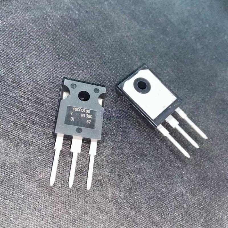
Image for reference only

Manufacturer Part:

VS-40CPQ100-N3

Package:

TO-247AC 3L (3-lead through-hole, 15.5mm width, tab for heatsink, common cathode configuration)

Brand:

Product Categories:

Quality Commitment

Shipping & Payment

Service & Packaging

Product Manual

Description

Product Overview

The VS-40CPQ100-N3 is a high-performance Schottky barrier rectifier from Vishay Semiconductors, featuring two 20 A diodes in a common-cathode configuration housed in a TO-247AC 3-lead package. With a total average forward current rating of 40 A and a reverse voltage of 100 V, this device is optimized for low forward voltage drop and high-frequency operation.

Fabricated using Vishay’s proprietary Schottky barrier technology with a guard ring structure for enhanced ruggedness and long-term reliability, the VS-40CPQ100-N3 features a forward voltage drop of typically 0.61 V per leg at 20 A and 125 degC. The device is capable of reliable operation up to 175 degC junction temperature, thanks to high-purity, high-temperature epoxy encapsulation that provides enhanced mechanical strength and moisture resistance.

This center-tap (common-cathode) Schottky rectifier is ideal for output rectification in switching power supplies, DC-DC converters, freewheeling diode applications, and reverse battery protection circuits. The -N3 suffix indicates halogen-free, RoHS-compliant construction with 100% lead-free terminations. The dual-diode common-cathode configuration simplifies center-tapped transformer output rectifier designs.

Key Specifications

Parameter Value
Average Forward Current (per leg) 20 A (40 A total, 50% duty cycle)
Peak Repetitive Reverse Voltage (VRRM) 100 V
Forward Voltage Drop (per leg) 0.61 V typ @ 20 A, TJ = 125 degC
Forward Voltage @ 25 degC (per leg) 0.77 V typ @ 20 A
Surge Current (IFSM, per leg) 2950 A (5 us sine) / 300 A (10 ms)
Reverse Leakage Current (per leg) 15 mA max @ TJ = 125 degC, VR = 100 V
Avalanche Energy (EAS, per leg) 11.25 mJ
Junction Capacitance (per leg) 600 pF typ @ VR = 5 V
Circuit Configuration Dual diode, common cathode
Maximum Junction Temperature 175 degC
Operating Temperature Range -55 degC to +175 degC
Thermal Resistance RthJC (per leg) 1.25 degC/W
Thermal Resistance RthJC (total) 0.63 degC/W
Package TO-247AC 3L
Recovery Type Schottky (majority carrier, effectively zero trr)

Features

  • Dual 20 A Schottky rectifiers, common cathode configuration (total 40 A)
  • 100 V reverse voltage rating
  • Very low forward voltage drop: 0.61 V typ @ 20 A, 125 degC
  • High temperature operation: TJ up to 175 degC
  • Ultra-fast switching (majority carrier device, no recovery tail)
  • High frequency operation capability
  • Guard ring for enhanced ruggedness and reliability
  • High surge current capability: 2950 A (5us)
  • Non-repetitive avalanche energy: 11.25 mJ
  • High purity, high temperature epoxy encapsulation
  • Enhanced mechanical strength and moisture resistance
  • Low series inductance: 7.5 nH per leg
  • dV/dt rating: 10,000 V/us
  • TO-247AC 3-lead through-hole package
  • Designed and qualified per JEDEC JESD 47
  • Halogen free, RoHS compliant, totally lead-free (-N3)

Applications

  • Output rectification in switching power supplies (SMPS)
  • DC-DC converters and POL regulators
  • Freewheeling and clamp diode applications
  • Reverse battery / reverse polarity protection
  • High-frequency DC-DC modules
  • Server and telecom power systems
  • Battery chargers and DC power distribution
  • High-efficiency low-voltage power supplies

Product Introduction: VS-40CPQ100-N3 Product Introduction

The VS-40CPQ100-N3 is a dual 20A Schottky barrier rectifier in a common-cathode configuration, providing a total current rating of 40A at 100V reverse voltage. Manufactured by Vishay Semiconductors, this device belongs to the high-performance Q-series Schottky product line, optimized for very low forward voltage drop while maintaining moderate reverse leakage at high temperatures.

Using proprietary Schottky barrier technology with a guard ring structure, the VS-40CPQ100-N3 achieves a forward voltage of typically only 0.61V per leg at 20A and 125 degC junction temperature. This exceptionally low VF translates directly into higher efficiency in power supply output rectifiers, where conduction losses are a significant portion of total power loss. The guard ring structure enhances device ruggedness and long-term reliability by suppressing edge effects and improving breakdown uniformity.

The TO-247AC 3-lead package houses two independent Schottky diodes sharing a common cathode connection. This configuration is particularly suited for center-tapped transformer full-wave rectifier circuits, push-pull converter output stages, and as parallel diodes when higher current capability is needed. The package provides low thermal resistance (0.63 degC/W for the whole package) when mounted to an appropriate heatsink.

Schottky diodes are majority-carrier devices with effectively zero reverse recovery time, making them ideal for high-frequency switching applications where recovery losses would otherwise significantly degrade efficiency. The -N3 suffix indicates Vishay’s halogen-free, RoHS-compliant, 100% lead-free product designation.

Working Principle: VS-40CPQ100-N3 Working Principle

The VS-40CPQ100-N3 Schottky rectifier operates on the principle of the Schottky barrier formed at a metal-semiconductor junction:

1. Schottky Barrier Formation: Unlike conventional PN-junction diodes, a Schottky diode is formed by the junction of a metal layer with a semiconductor (typically N-type silicon). The difference in work functions between the metal and semiconductor creates a rectifying barrier that allows current flow in one direction (from metal to semiconductor, i.e., anode to cathode) while blocking current in the reverse direction.

2. Forward Conduction: When forward-biased (anode positive, cathode negative), electrons in the N-type semiconductor easily surmount the Schottky barrier and flow into the metal contact. Since only majority carriers (electrons) are involved, there is no minority carrier injection or storage effect. The forward voltage drop is determined primarily by the barrier height and the series resistance of the drift region. At 20A and 125 degC, VF is typically 0.61V per leg.

3. Reverse Blocking: When reverse-biased, the Schottky barrier blocks electron flow from the metal back into the semiconductor. A small reverse leakage current flows due to thermionic emission over the barrier and tunneling effects. This leakage increases significantly with temperature (1.25mA at 25 degC rising to 15mA max at 125 degC). The 100V VRRM rating sets the maximum repetitive reverse voltage.

4. Zero Reverse Recovery: Because Schottky diodes are majority-carrier devices with no stored minority charge, they exhibit virtually zero reverse recovery time (trr). When switching from forward conduction to reverse blocking, the current stops almost instantaneously. This makes Schottky diodes far more efficient at high switching frequencies than PN-junction diodes, eliminating the losses and noise associated with reverse recovery.

5. Guard Ring Structure: The integrated guard ring is a PN junction formed around the perimeter of the Schottky contact. It reduces electric field crowding at the edges of the metal contact, improving breakdown voltage uniformity and long-term reliability. The guard ring also protects against surface-related failure mechanisms.

6. Thermal Considerations: With a maximum junction temperature of 175 degC, the VS-40CPQ100-N3 can operate at higher temperatures than standard silicon rectifiers. However, Schottky leakage current increases exponentially with temperature, so thermal design must ensure TJ stays within rated limits to prevent thermal runaway in continuous conduction modes. Proper heatsinking is essential.

Pin Description: VS-40CPQ100-N3 Pin Definition and Functions
Pin No. Pin Name Type Function
1 Anode 1 Anode Anode of first Schottky diode (Diode 1). Connect to first AC input in center-tap rectifier, or parallel with pin 3 for single-diode higher current operation.
2 Cathode (Common) Cathode Common cathode connection for both Schottky diodes. This is the positive output terminal in rectifier applications. Internally connected to the mounting tab.
3 Anode 2 Anode Anode of second Schottky diode (Diode 2). Connect to second AC input in center-tap rectifier configuration.
Tab Mounting Tab (Cathode) Thermal/Cathode Metal mounting tab is internally connected to the common cathode (pin 2). Bolt to heatsink. Use electrical insulation (mica pad, thermal pad) if the heatsink cannot be at cathode potential.

Package: TO-247AC 3L (3-lead through-hole plastic package). Body dimensions: ~15.5mm width x ~20.5mm length. Standard 0.1-inch (2.54mm) lead pitch. Large mounting tab for efficient thermal dissipation. Tab is at cathode (common) potential. Total weight approximately 6 grams.

Application Scenarios: In which products and applications is VS-40CPQ100-N3 used
  • Switching Power Supply Output Rectification: Secondary-side output rectifiers in forward, push-pull, and half-bridge SMPS topologies, where the low VF and zero recovery loss significantly improve overall efficiency, especially at high switching frequencies and low output voltages common in server, telecom, and datacom power supplies.
  • DC-DC Converter Freewheeling Diodes: Synchronous and non-synchronous buck converters, POL (point-of-load) regulators, and distributed power architectures, where Schottky diodes serve as freewheeling/clamp diodes or as backup diodes in parallel with synchronous MOSFETs to handle dead-time conduction and fault conditions.
  • Reverse Battery / Polarity Protection: Reverse polarity protection in automotive, telecom, and portable electronic systems, where the low VF of the Schottky diode minimizes power loss and voltage drop under normal operation while blocking reverse current if the power source is connected incorrectly.
  • High-Frequency DC-DC Modules: High-density DC-DC converter modules operating at frequencies from several hundred kHz to multi-MHz, where Schottky’s zero recovery characteristic is essential for maintaining efficiency and managing switching losses that would otherwise dominate at elevated frequencies.
  • Battery Charging Systems: Output rectifiers in battery chargers for consumer electronics, power tools, and industrial battery systems, where low forward voltage reduces heat generation and improves charge efficiency, especially in low-voltage battery chemistries like Li-ion and NiMH.
  • Server and Telecom Power Systems: High-efficiency server power supplies, telecom rectifiers, and -48V distributed power systems where energy efficiency and thermal management are critical design priorities, and the common-cathode dual configuration perfectly matches center-tapped transformer secondary windings.
  • OR-ing Diode Applications: N+1 power supply redundancy and load sharing applications where multiple power sources are ORed together, with the Schottky diode providing low-loss isolation between supply rails while preventing fault propagation from one supply to another.
  • Low-Voltage High-Current Power Supplies: Low output voltage (5V, 3.3V, and below) high-current power supplies where even small reductions in forward voltage drop translate into significant efficiency gains and thermal improvements that directly impact system reliability and cooling requirements.
Alternative Models: What chips are recommended as replacements for VS-40CPQ100-N3
Manufacturer Part Number IF/leg VRRM VF Typ Config Package
Vishay VS-40CPQ080-N3 20 A 80 V 0.55 V Common cathode TO-247-3
Vishay VS-60CPQ100-N3 30 A 100 V 0.67 V Common cathode TO-247-3
Vishay VS-40CTQ100-N3 20 A 100 V 0.70 V Common cathode TO-220-3
Onsemi MBR40100TG 20 A 100 V 0.68 V Common cathode TO-247-3
STMicro STPS40100CW 20 A 100 V 0.68 V Common cathode TO-247-3
Infineon IDB40E100 20 A 100 V 0.63 V Common cathode TO-247-3

Recommend Parts

ISO1176TDWR

Isolated RS-485 transceiver, 40Mbps, integrated transformer driver, SOIC-16

Brand: TI

Package: SOIC-16 (DW, wide-body, 10.3 x 10.3 mm)

IN STOCK: 6874pcs

Cargo cycle: 3-7 Days

The minimum order is 1

IRFB4020PBF

200V N-Channel HEXFET Power MOSFET, 31A, 68 mΩ RDS(on), TO-220AB

Brand: infineon

Package: TO-220AB

IN STOCK: 14149pcs

Cargo cycle: 3-7 Days

The minimum order is 1

NRF52832-QFAA-T

Nordic BLE SoC, ARM Cortex-M4 @ 64MHz, 64KB Flash, 32KB RAM, QFN-48

Package: See datasheet

IN STOCK: 10958pcs

Cargo cycle: 3-7 Days

The minimum order is 1

UCC28740DR

CVCC Flyback Controller, 700V startup, opto feedback, <10mW no-load, SOIC-7

Brand: TI

Package: SOIC-7 (4.9 x 3.9 x 1.75 mm)

IN STOCK: 4840pcs

Cargo cycle: 3-7 Days

The minimum order is 1

MMUN2211LT1G

NPN digital transistor, R1=10kΩ R2=10kΩ, 50V, 100mA, SOT-23-3, pre-biased BRT switch

Brand: Onsemi

Package: SOT-23-3 (TO-236, SC-59)

IN STOCK: 8500pcs

Cargo cycle: 3-7 Days

The minimum order is 1

TMS320F2810PBKA

C2000 Delfino DSP controller, 150MHz, 128KB Flash, BGA-179

Brand: TI

Package: BGA-179 (16 x 16 mm, PBK package)

IN STOCK: 3124pcs

Cargo cycle: 3-7 Days

The minimum order is 1




