






Opens in a new tab

XC6210B332MR-G

700mA LDO regulator, 3.3V fixed output, 220mV dropout, SOT-25-5, Torex XC6210B series, high ripple rejection, CE enable, ceramic cap stable

15400

Effective Inventory

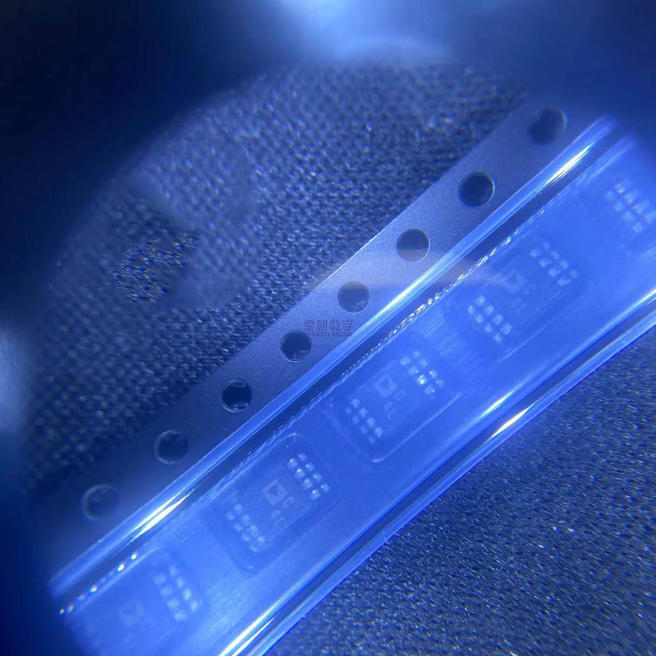
Image for reference only

Manufacturer Part:

XC6210B332MR-G

Package:

SOT-25 (5-pin SOT-23, 2.9×1.6×1.1mm body, 0.95mm pitch, surface mount)

Brand:

Quality Commitment

Shipping & Payment

Service & Packaging

Product Manual

Description

Product Overview

The XC6210B332MR-G is a high-speed, low-dropout (LDO) voltage regulator from Torex Semiconductor that provides a fixed 3.3 V output with up to 700 mA output current. This CMOS-based LDO features very low dropout voltage, high ripple rejection, and low quiescent current, making it ideal for battery-powered and portable applications.

The XC6210 series integrates a reference voltage source, error amplifier, phase compensation circuit, current limit circuit, foldback overcurrent protection, and a P-channel MOSFET output driver all on a single chip. The device operates from an input voltage range of 2.0 V to 6.0 V and delivers a fixed output voltage with +-2% accuracy. The 3.3 V version (B332) provides a typical dropout voltage of only 220 mV at 500 mA load current, ensuring efficient regulation even with low headroom.

Available in a small SOT-25 (SOT-25-5) surface-mount package, the XC6210B332MR-G features a built-in CE (chip enable) pin for turning the output on/off to save power. Additional features include inrush current suppression, output capacitor discharge function, and overcurrent foldback protection. The device is RoHS compliant and specified over the -40 degC to +85 degC operating temperature range.

Key Specifications

Parameter Value
Output Voltage 3.3 V fixed +-2%
Output Current 700 mA max
Input Voltage Range 2.0 V to 6.0 V
Dropout Voltage (Vdif) 220 mV typ @ 500 mA
Quiescent Current (Iq) 70 uA typ (ON state)
Standby Current 0.1 uA typ (CE = OFF)
Line Regulation 0.2% / V typical
Load Regulation 100 mV typical (10 mA to 500 mA)
Ripple Rejection 65 dB typical @ 1 kHz
Output Noise Voltage 90 uVrms typ (10 Hz to 100 kHz)
Short-Circuit Current Limit ~200 mA (foldback)
Current Limit 750 mA typ (constant current)
CE Pin Threshold 0.9 V typ (High = ON)
Output Capacitor 1.0 uF (ceramic compatible)
Operating Temperature -40 degC to +85 degC
Package SOT-25 (SOT-25-5, 5-pin SOT-23)

Features

  • 700 mA high output current low-dropout regulator
  • Fixed 3.3 V output with +-2% high accuracy
  • Low dropout voltage: 220 mV typ @ 500 mA
  • Wide input voltage range: 2.0 V to 6.0 V
  • Low quiescent current: 70 uA typical
  • Ultra-low standby current: 0.1 uA (CE off state)
  • High ripple rejection: 65 dB @ 1 kHz
  • Low output noise: 90 uVrms
  • Built-in CE (chip enable) function
  • Built-in output capacitor discharge function
  • Overcurrent protection with foldback current limit
  • Inrush current suppression during startup
  • Compatible with small ceramic output capacitors (1 uF)
  • P-channel MOS output driver
  • Stable with low ESR ceramic capacitors
  • SOT-25-5 small surface-mount package
  • RoHS compliant, lead-free, halogen-free
  • -40 degC to +85 degC operating temperature

Applications

  • Battery-powered equipment and portable devices
  • Mobile phones, smartphones, and wearables
  • Digital cameras and portable media players
  • Wireless communication modules
  • Microcontroller and logic power supplies
  • Post-regulation for switching power supplies
  • Reference voltage sources
  • Consumer electronics and home appliances

Product Introduction: XC6210B332MR-G Product Introduction

The XC6210B332MR-G is a 700mA high-output-current low-dropout (LDO) voltage regulator from Torex Semiconductor. Part of the XC6210 series of CMOS LDO regulators, this device is specifically designed for applications requiring high current capability in a small package with minimal external components.

With a fixed output voltage of 3.3V (accurate to +-2%), the XC6210B332MR-G can deliver up to 700mA of output current from an input supply ranging from 2.0V to 6.0V. The dropout voltage is typically only 220mV at 500mA output current, making it highly efficient even in low-headroom applications such as post-regulating a 3.7V Li-ion battery down to 3.3V.

The device integrates a P-channel MOSFET as the pass element, which provides both low dropout voltage and low quiescent current (70uA typical in operation). In standby mode (CE pin low), the supply current drops to just 0.1uA, making the device ideal for battery-powered applications where power conservation is critical.

Key protection features include overcurrent protection with foldback current limiting (which reduces the short-circuit current to approximately 200mA to prevent overheating), inrush current suppression during power-up to prevent input voltage dips, and a discharge function that actively discharges the output capacitor when the device is disabled.

The XC6210 is designed to be stable with a small 1uF ceramic output capacitor, eliminating the need for larger electrolytic capacitors and saving board space. The SOT-25-5 package (a 5-pin variant of the popular SOT-23) is one of the smallest packages available for this current rating, enabling compact PCB designs. The -MR-G suffix denotes the SOT-25 package (MR) in the green/lead-free version (-G).

Working Principle: XC6210B332MR-G Working Principle

The XC6210B332MR-G is a CMOS-based low-dropout linear regulator that maintains a constant output voltage by adjusting the resistance of a P-channel MOSFET pass element. Here’s how it works:

1. Reference Voltage: A precision bandgap voltage reference generates a stable, temperature-compensated reference voltage of approximately 0.8V. This reference is the voltage standard against which the output is compared and is designed to have near-zero temperature coefficient.

2. Voltage Divider: An internal resistive voltage divider samples a fraction of the output voltage. For the 3.3V version, the divider ratio is approximately 0.24 (0.8V reference / 3.3V output). The accuracy of this resistor divider directly contributes to the +-2% overall output voltage accuracy.

3. Error Amplifier: A high-gain CMOS error amplifier compares the divided output voltage with the reference voltage. Any difference generates an error signal that drives the gate of the P-channel MOSFET pass transistor. The error amplifier also includes phase compensation to ensure stability across all load conditions.

4. P-Channel MOSFET Pass Element: The pass transistor is a P-channel MOSFET connected between VIN and VOUT. When the output voltage drops below setpoint, the error amplifier reduces the gate voltage (more negative relative to source), turning the MOSFET more fully on and increasing the output current. When the output rises above setpoint, the gate voltage increases, turning the MOSFET off more and reducing output current.

5. Current Limit Circuit: A current sense element monitors the output current. If the current exceeds the limit threshold (approximately 750mA typical), the current limit circuit takes control of the gate drive and limits the output current. The foldback characteristic further reduces the current when the output is shorted to ground (down to ~200mA), protecting both the regulator and the load from damage.

6. CE (Chip Enable): The CE pin controls the on/off state of the regulator. When CE is above the threshold (0.9V typ), the regulator is enabled. When CE is low, the regulator is shut down, reducing supply current to 0.1uA. The CE pin is compatible with both 3.3V and 5V logic levels.

7. Discharge Function: When the regulator is disabled (CE = low), an internal discharge switch connects the output to ground, actively discharging the output capacitor. This ensures the output voltage falls quickly when the regulator is turned off, which is useful in applications where the output must be fully discharged before re-enabling.

8. Soft-Start / Inrush Control: During startup, an internal soft-start circuit gradually ramps up the output voltage, limiting the inrush current that charges the output capacitor and preventing dips on the input supply line.

Pin Description: XC6210B332MR-G Pin Definition and Functions
Pin No. Pin Name Type Function
1 VSS (GND) Ground Ground reference pin. Connect directly to ground plane for best performance and noise rejection.
2 CE Input Chip Enable input. High = regulator ON, Low = regulator OFF (standby). Logic high threshold ~0.9V. Can be tied directly to VIN for always-on operation. Active high: >0.9V turns on, <0.4V turns off.
3 NC – No Connection. For standard B-type, leave unconnected. Do not connect to ground or VCC.
4 VOUT Regulated Output Regulated 3.3V output. Connect a 1.0uF ceramic capacitor from this pin to VSS, placed as close as possible to the pin for stability and transient response.
5 VIN Power Input Unregulated input voltage (2.0V to 6.0V). Connect a 1.0uF (minimum) ceramic bypass capacitor from this pin to VSS, placed close to the device.

Package: SOT-25-5 (also known as SOT-25 or SOT-23-5). 5-pin small outline transistor package variant. Body dimensions: 2.9mm x 1.6mm x 1.1mm (typical height). 0.95mm pitch between leads. Surface-mount device. Tape and reel packaging (MR suffix).

Application Scenarios: In which products and applications is XC6210B332MR-G used
  • Battery-Powered Portable Devices: Power regulation for battery-operated equipment such as handheld meters, portable test instruments, GPS devices, and wearable electronics, where the combination of low quiescent current (70uA), ultra-low standby current (0.1uA), and low dropout voltage maximizes battery life across the discharge cycle.
  • Wireless Communication Modules: Clean power supply for Wi-Fi, Bluetooth, Zigbee, and cellular modules, where the high ripple rejection (65dB @1kHz) and low output noise (90uVrms) provide the low-noise supply rail required for sensitive RF circuits to maintain optimal sensitivity and transmission performance.
  • Microcontroller and Logic Power Supplies: 3.3V power supply for microcontrollers, FPGAs, CPLDs, memory chips, and other digital ICs in embedded systems, where the 700mA current rating provides sufficient headroom for typical MCU-based designs and the small SOT-25 package minimizes board space.
  • Post-Regulation for Switching Power Supplies: Secondary LDO regulation following a switching DC-DC converter, where the XC6210 removes switching ripple and noise from the switcher output to provide clean analog or RF supply rails, leveraging its excellent ripple rejection performance to achieve very low output noise.
  • Mobile and Wearable Electronics: Power supply for smartphones, smart watches, fitness trackers, and wireless earbuds, where the small SOT-25 footprint, low quiescent current, and CE pin for power gating enable efficient power management in space-constrained, battery-operated consumer devices.
  • Digital Cameras and Portable Media: Multiple supply rails in digital cameras, portable media players, and handheld gaming devices, providing regulated power for image sensors, audio codecs, display drivers, and memory circuits, with the inrush suppression feature ensuring clean power-up sequencing.
  • Reference Voltage Sources: Providing stable, low-noise reference voltages for ADCs, DACs, sensor signal conditioning, and precision analog circuits, where the low output noise and high line rejection ensure that reference voltage variations do not degrade measurement accuracy.
  • Consumer Electronics and Home Appliances: Power regulation in set-top boxes, smart home devices, small appliances, and LED drivers, where the low cost, small package, and minimal external components (just two capacitors) make it ideal for high-volume, cost-sensitive consumer applications.
Alternative Models: What chips are recommended as replacements for XC6210B332MR-G
Manufacturer Part Number Vout Iout Dropout Iq Package
Torex XC6206P332MR 3.3 V 200 mA 170 mV 1.0 uA SOT-23
Torex XC6210B182MR-G 1.8 V 700 mA 180 mV 70 uA SOT-25
Torex XC6210B502MR-G 5.0 V 700 mA 260 mV 70 uA SOT-25
TI TPS73633 3.3 V 400 mA 220 mV 350 uA SOT-23
Microchip MCP1700-3302E 3.3 V 250 mA 178 mV 1.6 uA SOT-23
RICOH R1114D331B 3.3 V 500 mA 200 mV 65 uA SOT-25

Recommend Parts

ISO1176TDWR

Isolated RS-485 transceiver, 40Mbps, integrated transformer driver, SOIC-16

Brand: TI

Package: SOIC-16 (DW, wide-body, 10.3 x 10.3 mm)

IN STOCK: 6874pcs

Cargo cycle: 3-7 Days

The minimum order is 1

IRFB4020PBF

200V N-Channel HEXFET Power MOSFET, 31A, 68 mΩ RDS(on), TO-220AB

Brand: infineon

Package: TO-220AB

IN STOCK: 14149pcs

Cargo cycle: 3-7 Days

The minimum order is 1

NRF52832-QFAA-T

Nordic BLE SoC, ARM Cortex-M4 @ 64MHz, 64KB Flash, 32KB RAM, QFN-48

Package: See datasheet

IN STOCK: 10958pcs

Cargo cycle: 3-7 Days

The minimum order is 1

UCC28740DR

CVCC Flyback Controller, 700V startup, opto feedback, <10mW no-load, SOIC-7

Brand: TI

Package: SOIC-7 (4.9 x 3.9 x 1.75 mm)

IN STOCK: 4840pcs

Cargo cycle: 3-7 Days

The minimum order is 1

MMUN2211LT1G

NPN digital transistor, R1=10kΩ R2=10kΩ, 50V, 100mA, SOT-23-3, pre-biased BRT switch

Brand: Onsemi

Package: SOT-23-3 (TO-236, SC-59)

IN STOCK: 8500pcs

Cargo cycle: 3-7 Days

The minimum order is 1

TMS320F2810PBKA

C2000 Delfino DSP controller, 150MHz, 128KB Flash, BGA-179

Brand: TI

Package: BGA-179 (16 x 16 mm, PBK package)

IN STOCK: 3124pcs

Cargo cycle: 3-7 Days

The minimum order is 1




