






Opens in a new tab

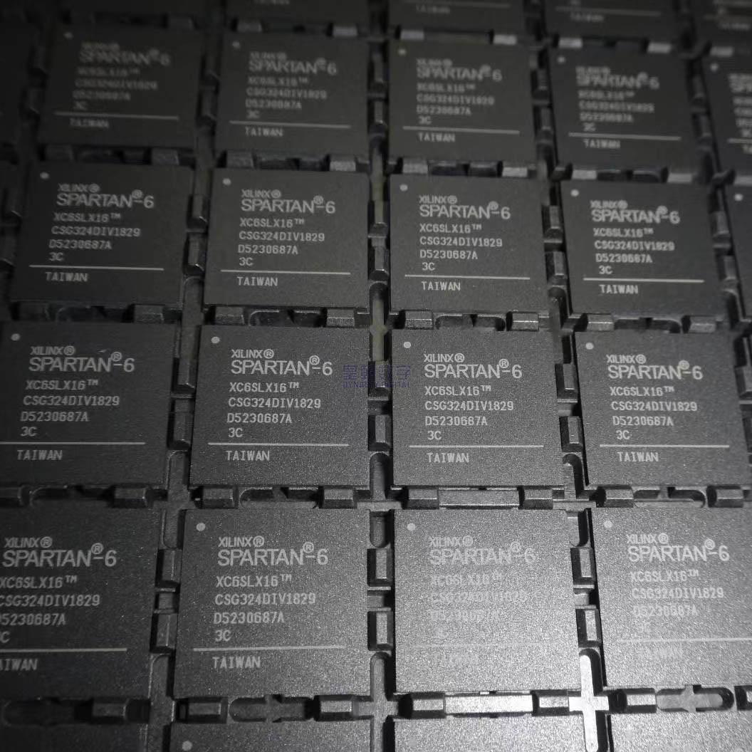
XC6SLX16-2CSG324C

Spartan-6 LX FPGA, 14579 logic cells, 32 DSP, 576KB RAM, 232 I/O, 45nm, CSBGA-324, -2 speed, commercial 0-85 degC, Xilinx/AMD

1850

Effective Inventory

Image for reference only

Manufacturer Part:

XC6SLX16-2CSG324C

Package:

CSG324 (324-pin chip-scale BGA, 15x15mm body, 0.8mm ball pitch, 18×18 ball array, 4 banks)

Brand:

Quality Commitment

Shipping & Payment

Service & Packaging

Product Manual

Description

Product Overview

The XC6SLX16-2CSG324C is a member of the Xilinx Spartan-6 family of low-cost FPGAs, offering 14,579 logic cells in a 324-pin chip-scale BGA (CSBGA) package. Manufactured on a mature 45 nm low-power copper process technology, the Spartan-6 family delivers optimal balance of cost, power, and performance for high-volume applications.

The XC6SLX16 device features 2,278 configurable logic blocks (CLBs) with 18,224 flip-flops, 32 DSP48A1 slices for signal processing, and 32 block RAMs totaling 576 Kb of embedded memory. It includes two Clock Management Tiles (CMTs), each containing two DCMs and one PLL for flexible clock generation and management. An integrated memory controller block supports DDR, DDR2, DDR3, and LPDDR interfaces with data rates up to 800 Mb/s.

Housed in a CSG324 (CSBGA-324) package measuring 15 x 15 mm, the XC6SLX16-2CSG324C provides up to 232 user I/O pins distributed across 4 I/O banks, supporting over 40 different I/O standards including LVCMOS, LVTTL, HSTL, SSTL, and LVDS. The -2 speed grade provides high performance with commercial temperature range (0 degC to 85 degC). Ideal applications include cost-sensitive bridging, industrial automation, automotive infotainment, and consumer electronics.

Key Specifications

Parameter Value
Logic Cells 14,579
CLB Slices 2,278 (569 SLICEM + 1,709 SLICEL)
Flip-Flops 18,224
Distributed RAM 136 Kb max
Block RAM (18 Kb each) 32 blocks (576 Kb total)
DSP48A1 Slices 32 (18×18 multiplier + adder + accumulator)
Clock Management Tiles (CMT) 2 (each: 2 DCMs + 1 PLL)
Memory Controller Blocks 2 (DDR/DDR2/DDR3/LPDDR, up to 800 Mb/s)
GTP Transceivers 0 (LX variant, no serial transceivers)
PCIe Endpoint Block 0 (LX variant)
I/O Banks 4 banks
Max User I/Os (CSG324) 232 single-ended / 106 differential pairs
Max I/O Data Rate (diff) 1,080 Mb/s per LVDS pair
Core Voltage 1.2 V (1.14-1.26 V)
Speed Grade -2 (commercial)
Configuration SPI x1/x2/x4, BPI, JTAG, MultiBoot
Package CSG324 (CSBGA, 15×15 mm, 0.8 mm pitch)
Operating Temperature 0 degC to +85 degC (commercial)

Features

  • Spartan-6 LX FPGA: optimized for low cost logic applications
  • 14,579 logic cells with 6-input LUT architecture
  • 32 DSP48A1 slices for high-performance arithmetic
  • 576 Kb block RAM + 136 Kb distributed RAM
  • 2 CMTs with DCMs and PLLs for flexible clocking
  • 2 integrated memory controller blocks (DDR2/DDR3)
  • Up to 232 user I/O pins (CSG324 package)
  • 40+ I/O standards: LVCMOS, LVTTL, HSTL, SSTL, LVDS
  • SelectIO technology with adjustable slew and drive
  • Hot swap compliance on I/O banks
  • 8 low-skew global clock networks per CMT
  • Device DNA unique identifier for design authentication
  • Advanced power management: suspend, hibernate modes
  • MultiBoot support for remote upgrades with watchdog
  • 45 nm low-power copper process technology
  • MicroBlaze soft processor support
  • ISE Design Suite development tools
  • Long product lifecycle: supported through at least 2030
  • RoHS compliant, lead-free CSBGA package

Applications

  • Industrial automation and factory networking
  • Automotive infotainment and display systems
  • Cost-sensitive bridging and interface conversion
  • Consumer electronics and set-top boxes
  • Video processing and display control
  • Motor control and motion systems
  • Communication and data bridging
  • Medical and healthcare equipment
Product Introduction: XC6SLX16-2CSG324C Product Introduction

The XC6SLX16-2CSG324C is a mid-density member of Xilinx’s (now AMD) Spartan-6 LX family of cost-optimized FPGAs. Built on a mature 45nm low-power copper process, this device provides 14,579 logic cells in a compact 324-ball chip-scale BGA package, delivering an excellent balance of performance, features, and cost for high-volume applications.

At the heart of the Spartan-6 architecture is an efficient 6-input LUT (look-up table) with dual flip-flops, enabling both high combinational logic performance and efficient pipelined designs. The 14,579 logic cells are organized into 2,278 CLB slices – approximately 25% are SLICEMs capable of implementing distributed RAM and shift registers (SRL), while the remaining 75% are SLICEL/SLICEX for general logic.

For digital signal processing applications, 32 DSP48A1 slices provide dedicated 18×18-bit multipliers with integrated adders and accumulators, supporting efficient FIR filters, FFT accelerators, and other DSP functions at significantly higher performance than logic-only implementations. Memory resources include 32 block RAMs (18Kb each, splittable into two 9Kb blocks) totaling 576Kb, plus up to 136Kb of distributed RAM implemented in SLICEM LUTs.

Clock management is handled by two Clock Management Tiles (CMTs), each containing two Digital Clock Managers (DCMs) for clock skew elimination and frequency synthesis, plus one Phase-Locked Loop (PLL) for low-jitter clock generation and phase shifting. Two integrated memory controller blocks support DDR, DDR2, DDR3, and LPDDR interfaces at data rates up to 800Mb/s, providing high-bandwidth memory access without consuming general-purpose FPGA logic.

The CSG324 package provides 232 user I/O pins across four I/O banks, supporting over 40 I/O standards including LVCMOS (1.2V-3.3V), LVTTL, HSTL, SSTL, and LVDS (up to 106 differential pairs). The -2 speed grade provides the second-highest performance level for commercial temperature (0 degC to 85 degC) operation. AMD has announced long-term support for Spartan-6 devices through at least 2030, ensuring supply stability for long-lifecycle programs.

Working Principle: XC6SLX16-2CSG324C Working Principle

The Spartan-6 XC6SLX16 FPGA is a programmable logic device that can be configured to implement virtually any digital logic function. Here are the key aspects of its architecture and operation:

1. Configurable Logic Blocks (CLBs): The fundamental logic resource. Each CLB contains two slices, and each slice contains four 6-input LUTs, eight flip-flops, carry logic for arithmetic, and multiplexer logic. SLICEM slices (25% of total) can additionally implement distributed RAM (64-bit per LUT) or shift registers (SRL32/SRL16). The 6-input LUT can implement any 6-input, 1-output Boolean function, or split into two 5-input, 2-output functions with common inputs.

2. Block RAM: 32 dedicated 18Kb memory blocks arranged in columns. Each block can be configured as a single 18Kb RAM or two independent 9Kb RAMs. They support true dual-port, simple dual-port, and single-port modes with byte write enables. Block RAMs can be cascaded to create larger memories. They operate at the full fabric speed for high-bandwidth data buffering and storage.

3. DSP48A1 Slices: 32 dedicated arithmetic blocks arranged in a column. Each DSP48A1 contains an 18×18-bit two’s complement multiplier, a 48-bit accumulator, and a pre-adder. They support pipelining for high clock rates and cascading for wider arithmetic operations. DSP slices can implement multipliers, multiply-accumulate (MAC), adders, subtractors, and comparators at much higher efficiency than LUT-based implementations.

4. Clock Management Tiles (CMTs): Two CMTs provide comprehensive clock generation and management. Each CMT contains two DCMs (Digital Clock Managers) for duty-cycle correction, phase shifting, frequency synthesis, and deskew; plus one PLL (Phase-Locked Loop) for low-jitter clock multiplication and phase alignment. Sixteen global clock networks distribute clocks across the device with minimal skew.

5. Memory Controller Blocks (MCBs): Two hard memory controller blocks provide dedicated, high-performance interfaces to external DRAM. They support DDR, DDR2, DDR3, and LPDDR memory types with data rates up to 800Mb/s (12.8 Gb/s peak bandwidth per MCB). The MCB includes a multi-port bus architecture with independent FIFOs, easing timing closure in user designs.

6. SelectIO I/O Banks: Four I/O banks surround the logic fabric. Each bank has its own Vcco supply voltage, enabling mixed-voltage designs. The IOBs (I/O Blocks) can be configured for single-ended or differential signaling with programmable termination, drive strength (up to 24mA), and slew rate. Supported standards include LVCMOS, LVTTL, HSTL, SSTL, LVDS, and more.

7. Configuration: The FPGA loads its configuration from an external non-volatile memory (SPI Flash, NOR Flash) at power-up via dedicated configuration pins or JTAG. The configuration bitstream programs all LUTs, flip-flops, block RAMs, DSP slices, IOBs, and routing to implement the desired digital circuit. MultiBoot supports loading multiple bitstreams for remote updates with watchdog protection.

8. Power Management: Multiple power-saving modes are available including Suspend (maintains configuration and state, multi-pin wakeup) and Hibernate (zero power, state lost). Normal operating power is reduced by the 45nm process and optimized architecture compared to previous FPGA generations.

Pin Description: XC6SLX16-2CSG324C Pin Definition and Functions
Pin Group Description
VCCINT Core power supply: 1.2 V (1.14 V to 1.26 V). Multiple VCCINT balls distributed across the package. All must be connected.
VCCAUX Auxiliary power supply: 2.5 V. Powers clock management, configuration logic, and other auxiliary circuits.
VCCBANKx I/O bank supply voltages. 4 banks total (Bank 0, 1, 2, 3). Each bank can have a different Vcco voltage (1.2V to 3.3V).
GND Ground balls. Numerous ground pins distributed throughout the package for signal integrity and power distribution.
User I/O (IO_LxxP/N) General-purpose user I/O pins. Up to 232 single-ended I/O or 106 LVDS differential pairs. Each pin can be configured as input, output, or bidirectional.
MRCC/SRCC Clock-capable I/O pins (Multi-Region / Single-Region Clock Capable). For external clock inputs with optimized routing to CMTs.
Configuration Pins CCLK (configuration clock), D0-D7 (configuration data), DIN, DOUT, CSI_B, RDWR_B, INIT_B, DONE, PROGRAM_B, M0, M1, M2 (mode pins).
JTAG Pins TCK (test clock), TMS (test mode select), TDI (test data in), TDO (test data out). IEEE 1149.1 boundary scan and FPGA configuration.
POWER_BTN Multi-pin wake-up control pin for Suspend mode (when enabled in bitstream).
SUSPEND Suspend mode control input. Active high to enter suspend mode with state retention.
AWAKE Wake status output. Indicates device is awake from suspend mode.

Package: CSG324 – Chip-Scale Ball Grid Array, 324 balls. Package dimensions: 15mm x 15mm body size. Ball pitch: 0.8mm. Ball array: approximately 18×18 grid. 4 I/O banks. Commercial grade, 0 degC to 85 degC operating range.

Application Scenarios: In which products and applications is XC6SLX16-2CSG324C used
  • Industrial Automation and Control: PLC modules, industrial Ethernet bridges, motor controllers, and factory I/O systems, where the FPGA’s flexibility enables custom interface protocols, real-time processing, and integration of multiple functions (logic, DSP, memory, I/O) in a single chip, reducing BOM cost and board space.
  • Automotive Infotainment and Displays: Display controllers, video scaling, touch processing, and infotainment interfaces in automotive head units and instrument clusters, where the Spartan-6’s cost optimization, video capability, and long product lifecycle align with automotive program requirements and extended supply guarantees through 2030.
  • Cost-Sensitive Interface Bridging: Protocol conversion and bridging applications such as PCIe to local bus, LVDS to CMOS, camera interface bridging, and multi-protocol communication adapters, leveraging the 232 I/O pins and 40+ I/O standards for flexible interface design with minimal external logic.
  • Consumer Electronics and Set-Top Boxes: Video processing, display control, and system glue logic in set-top boxes, digital TVs, media players, and gaming accessories, where the combination of DSP slices, block RAM, and I/O flexibility enables efficient implementation of video pipelines and system interfaces at low cost.
  • Video Processing and Display: Low-cost video scaling, deinterlacing, overlay, and display timing control for LCD/OLED panels, video surveillance cameras, and digital signage, using block RAM for line buffers and DSP slices for pixel processing operations.
  • Motor Control and Motion Systems: FPGA-based motor controllers for servo drives, stepper motors, and multi-axis motion systems, where the DSP slices implement current control loops, PWM generation, and encoder interface processing in hardware for deterministic real-time performance.
  • Medical and Healthcare Equipment: Ultrasound, patient monitoring, diagnostic instruments, and laboratory equipment requiring signal processing, high-speed data acquisition, and flexible I/O interfaces, with the FPGA providing hardware acceleration for DSP algorithms and real-time data path management.
  • Communication and Data Acquisition: Multi-channel data acquisition systems, software-defined radio front-ends, and industrial communication adapters, where the integrated memory controllers provide high-bandwidth buffer memory and the SelectIO technology enables interfacing with various data converters and communication PHYs.
Alternative Models: What chips are recommended as replacements for XC6SLX16-2CSG324C
Manufacturer Part Number Logic Cells DSP BRAM I/O Package Notes
Xilinx/AMD XC6SLX9-2CSG324C 9,152 16 576 Kb 200 CSG324 Smaller, same package
Xilinx/AMD XC6SLX25-2CSG324C 24,051 38 936 Kb 266 CSG324 Larger, same package
Xilinx/AMD XC6SLX16-2FTG256C 14,579 32 576 Kb 200 FTBGA-256 Same die, smaller BGA
Intel/Altera EP4CE15F23C8N 15,408 LE 56 M9K 504 Kb 179 BGA-256 Cyclone IV E competitor
Lattice LFE5UM-25F-8BG381C 24 K LUT 28 DSP 900 Kb 224 caBGA-381 ECP5, newer generation
Gowin GW2A-LV18PG256C6 20 K LUT 48 DSP 415 Kb 168 PBGA-256 Chinese alternative, low cost

Recommend Parts

ISO1176TDWR

Isolated RS-485 transceiver, 40Mbps, integrated transformer driver, SOIC-16

Brand: TI

Package: SOIC-16 (DW, wide-body, 10.3 x 10.3 mm)

IN STOCK: 6874pcs

Cargo cycle: 3-7 Days

The minimum order is 1

IRFB4020PBF

200V N-Channel HEXFET Power MOSFET, 31A, 68 mΩ RDS(on), TO-220AB

Brand: infineon

Package: TO-220AB

IN STOCK: 14149pcs

Cargo cycle: 3-7 Days

The minimum order is 1

NRF52832-QFAA-T

Nordic BLE SoC, ARM Cortex-M4 @ 64MHz, 64KB Flash, 32KB RAM, QFN-48

Package: See datasheet

IN STOCK: 10958pcs

Cargo cycle: 3-7 Days

The minimum order is 1

UCC28740DR

CVCC Flyback Controller, 700V startup, opto feedback, <10mW no-load, SOIC-7

Brand: TI

Package: SOIC-7 (4.9 x 3.9 x 1.75 mm)

IN STOCK: 4840pcs

Cargo cycle: 3-7 Days

The minimum order is 1

MMUN2211LT1G

NPN digital transistor, R1=10kΩ R2=10kΩ, 50V, 100mA, SOT-23-3, pre-biased BRT switch

Brand: Onsemi

Package: SOT-23-3 (TO-236, SC-59)

IN STOCK: 8500pcs

Cargo cycle: 3-7 Days

The minimum order is 1

TMS320F2810PBKA

C2000 Delfino DSP controller, 150MHz, 128KB Flash, BGA-179

Brand: TI

Package: BGA-179 (16 x 16 mm, PBK package)

IN STOCK: 3124pcs

Cargo cycle: 3-7 Days

The minimum order is 1





