






Opens in a new tab

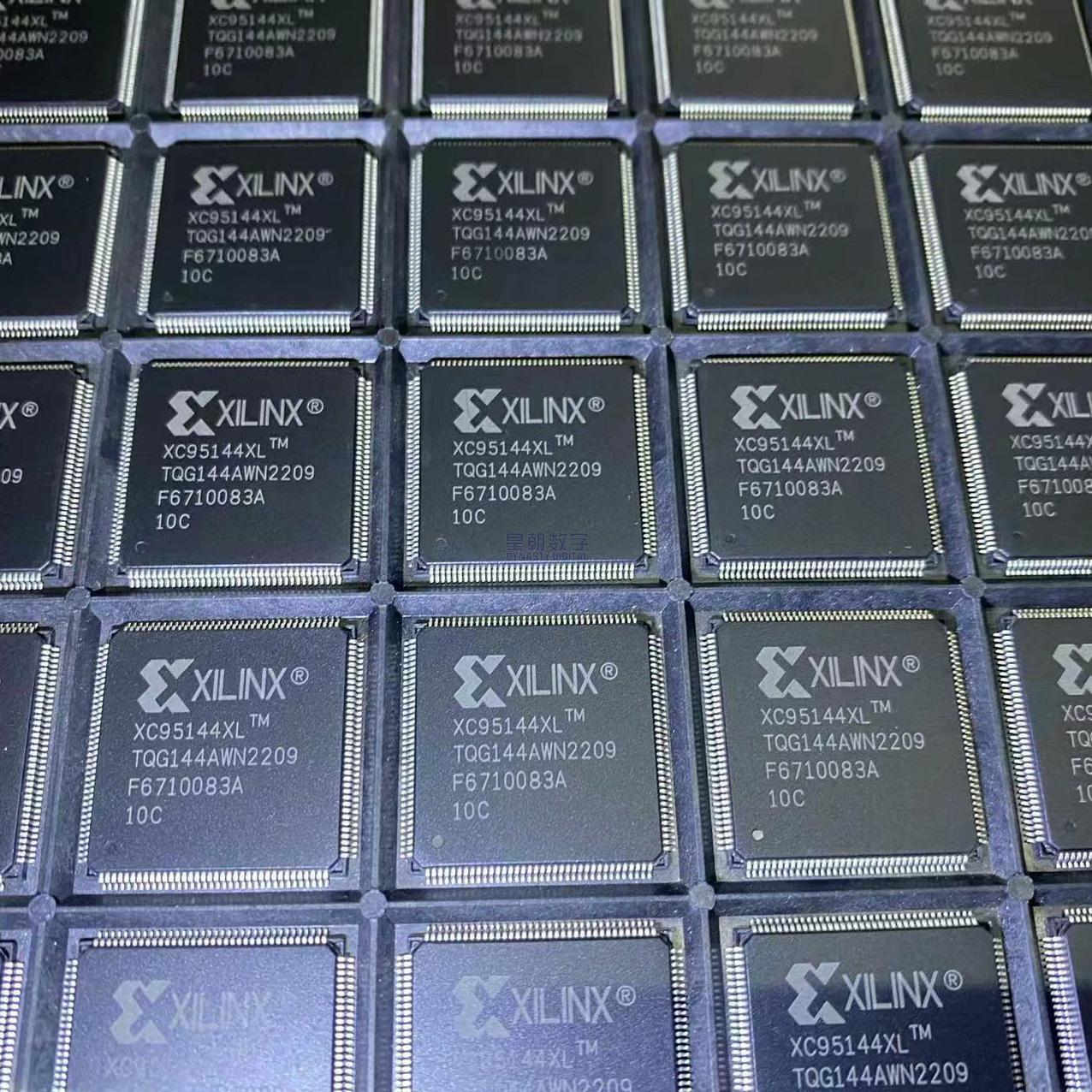
XC95144XL-TQG144AW

XC9500XL CPLD, 144 macrocells, 3200 gates, 5ns tPD, 178MHz, 117 I/O, TQFP-144 22x22mm, 3.3V, 5V tolerant, automotive -40~125C, AMD Xilinx

1680

Effective Inventory

Image for reference only

Manufacturer Part:

XC95144XL-TQG144AW

Package:

TQG144 (144-pin thin quad flat pack, 22x22mm body, 0.5mm lead pitch, 4-sided gull-wing leads, lead-free)

Brand:

Quality Commitment

Shipping & Payment

Service & Packaging

Product Manual

Description

Product Overview

The XC95144XL-TQG144AW is a high-performance CPLD from Xilinx (AMD) featuring 144 macrocells in a 144-pin Thin Quad Flat Pack (TQFP) package. Part of the XC9500XL family of 3.3 V CPLDs built on advanced 0.35 micron CMOS FastFLASH technology, this device delivers 5 ns pin-to-pin logic delays with system frequencies up to 178 MHz.

The XC95144XL provides 3,200 usable gates and 144 macrocells organized in multiple 54-input Function Blocks (FBs) connected by the FastCONNECT II switch matrix. Each macrocell features up to 90 product terms with individual product-term allocation, a flip-flop/latch, and independent clock and output enable control. The architecture provides superior pin-locking capability, meaning design changes do not require board rework as long as I/O assignments remain stable.

The TQG144 package provides 117 user I/O pins, supporting 5 V tolerant inputs and 3.3 V or 2.5 V output operation. Advanced system features include in-system programming (ISP) via JTAG, individual output slew rate control, input hysteresis on all user pins, bus-hold circuitry, hot-plugging support, and full IEEE 1149.1 boundary-scan. The device offers enhanced data security and excellent reliability with 10,000 program/erase cycles endurance and 20-year data retention. The -AW suffix indicates extended/automotive grade temperature range.

Key Specifications

Parameter Value
Macrocells 144
Usable Gates 3,200
Registers 144
Function Blocks 8 (54 inputs each)
Product Terms per FB 90 per macrocell, shared (up to 90 per macrocell via allocator)
Pin-to-Pin Delay (tPD) 5 ns typical (-10 speed grade)
Setup Time (tSU) 3.7 ns
Clock to Output (tCO) 3.5 ns
System Frequency (fSYSTEM) 178 MHz
Global Clock Pins 3 (GCK1, GCK2, GCK3)
Global OE Pins 4 (GTS1-GTS4)
Global Set/Reset 1 (GSR)
User I/O Pins (TQ144) 117
Supply Voltage (VCCINT) 3.0 V to 3.6 V (3.3 V nominal)
I/O Supply (VCCIO) 2.5 V or 3.3 V
Input Tolerance 5 V tolerant
Output Standards 3.3 V LVTTL, 2.5 V CMOS
Programming In-System Programmable via JTAG (IEEE 1149.1)
Endurance 10,000 program/erase cycles minimum
Data Retention 20 years minimum
Operating Temperature -40 degC to +125 degC (automotive Q-grade, AW suffix)
Package TQG144 / TQFP-144 (22 x 22 mm, 0.5 mm pitch)

Features

  • 144 macrocells, 3,200 usable gates, 5 ns pin-to-pin delay
  • FastFLASH 0.35 micron CMOS technology
  • Optimized for high-performance 3.3 V systems
  • 5 V tolerant I/O pins (accept 5V, 3.3V, 2.5V signals)
  • 3.3 V or 2.5 V output capability
  • Superior pin-locking with FastCONNECT II switch matrix
  • Extra wide 54-input Function Blocks
  • Up to 90 product-terms per macrocell with individual allocation
  • 3 global clock pins + product-term clocks (local inversion)
  • 4 global output enables with local inversion
  • Global set/reset (GSR)
  • Input hysteresis on all user and JTAG inputs
  • Bus-hold circuitry on all user pin inputs
  • Hot-plugging capability
  • Full IEEE 1149.1 JTAG boundary-scan support
  • In-system programmable (ISP)
  • Fast concurrent programming
  • Slew rate control on individual outputs
  • Enhanced data security features
  • 10,000+ program/erase cycles
  • 20-year data retention
  • Pin-compatible with 5 V core XC95144 family
  • TQFP-144 package, lead-free, RoHS compliant
  • Extended automotive temperature range

Applications

  • Automotive electronics and ADAS systems
  • Industrial control and factory automation
  • Telecommunications and networking equipment
  • High-speed address decoding and glue logic
  • Bus bridging and protocol conversion
  • Power supply control and sequencing
  • High-speed interconnect and switching
  • Field upgrades and reconfigurable logic

Product Introduction: XC95144XL-TQG144AW Product Introduction

The XC95144XL-TQG144AW is a 144-macrocell CPLD from Xilinx’s XC9500XL family, offering high-performance 3.3V operation in a 144-pin Thin QFP package. The -AW suffix denotes extended/automotive grade temperature operation (-40 degC to +125 degC), making this device suitable for demanding automotive and high-temperature industrial applications.

Built on Xilinx’s proven FastFLASH CMOS technology (0.35 micron feature size), the XC95144XL delivers 5 ns pin-to-pin logic delays with system frequencies up to 178 MHz. The device contains 144 macrocells providing approximately 3,200 usable gates, organized in eight Function Blocks (FBs) interconnected by the FastCONNECT II switch matrix. Each FB has 54 inputs and 18 macrocells (in the XC95144XL configuration), with up to 90 product terms available per macrocell through an intelligent product term allocator.

A key advantage of the XC9500XL architecture is superior pin-locking capability. Because of the wide 54-input Function Blocks and flexible product term allocation, design changes typically do not affect pin assignments, eliminating the need for costly PCB rework. This is especially valuable for long-lifecycle programs where logic updates may be required after production has started.

The TQFP-144 package provides 117 user I/O pins, the maximum I/O count available for the XC95144XL device. I/Os support 5V tolerance on inputs, enabling seamless interfacing with legacy 5V systems, while outputs operate at either 3.3V or 2.5V levels. All outputs feature individually programmable slew rate control for managing signal integrity and electromagnetic interference.

In-system programming (ISP) via the standard JTAG interface allows device programming after the CPLD is soldered to the board, enabling field upgrades and manufacturing test flexibility. The device supports 10,000+ program/erase cycles with 20-year data retention, ensuring reliable operation over the product lifetime. The XC95144XL is pin-compatible with the 5V-core XC95144 device in common packages, simplifying migration from 5V to 3.3V designs.

Working Principle: XC95144XL-TQG144AW Working Principle

The XC95144XL is a Complex Programmable Logic Device (CPLD) based on Flash EEPROM technology. Here is how its architecture works:

1. Function Blocks (FBs): The device is divided into eight Function Blocks, each containing 18 macrocells and associated product term arrays. Each FB has 54 inputs coming from the FastCONNECT II switch matrix. The wide input structure (54 inputs per FB) reduces the need for inter-block routing, which is a key factor in maintaining consistent pin-to-pin delays and achieving excellent pin-locking performance.

2. Macrocell Architecture: Each macrocell consists of:
– A sum-of-products (AND-OR) logic structure with five direct product terms
– A product term allocator that can reassign up to 90 product terms from other macrocells in the same FB to a single macrocell requiring more logic
– A programmable flip-flop/latch with individual clock, set, and reset controls
– An output enable multiplexer (global OE or product-term OE)
– Output polarity control (inverting or non-inverting)
The flip-flop can be configured as D-type, T-type, JK, or SR, or bypassed for combinatorial outputs.

3. FastCONNECT II Switch Matrix: This is the central routing resource that connects all I/O blocks and Function Block outputs to the Function Block inputs. It provides fully predictable, uniform routing delays regardless of which pins are used. This deterministic timing model simplifies timing analysis and ensures that performance does not degrade with design changes (pin-locking guarantee).

4. I/O Blocks (IOBs): Each IOB connects the internal logic to the external package pin. Features include:
– Input buffer with hysteresis (Schmitt trigger) for improved noise immunity
– Output driver with programmable slew rate (fast or slow)
– Bus-hold circuitry (eliminates need for pull-up/pull-down resistors on unused inputs)
– Output enable control (from global OE pins or product-term logic)
– 5V tolerance on inputs (accepts 5V, 3.3V, and 2.5V signals)
– Output voltage determined by VCCIO (3.3V or 2.5V)

5. Global Signals: Three global clock pins (GCK1-3) provide low-skew clock distribution across the device. Four global output enable pins (GTS1-4) enable/disable output buffers. One global set/reset (GSR) pin can initialize all flip-flops. All global signals can also be driven by internal product-term logic.

6. JTAG / ISP: The JTAG interface (TCK, TMS, TDI, TDO) supports both boundary-scan testing per IEEE 1149.1 and in-system programming. Programming is done through the same JTAG port, eliminating the need for a separate programming interface. Fast concurrent programming allows the entire device to be programmed in seconds.

7. FastFLASH Technology: The configuration is stored in non-volatile Flash EEPROM cells distributed throughout the device. Unlike SRAM-based FPGAs, CPLDs do not require external configuration memory – they are live at power-up. The Flash cells are rated for 10,000+ program/erase cycles and 20-year data retention.

Pin Description: XC95144XL-TQG144AW Pin Definition and Functions
Pin Group Pin Name(s) Type Description
Power VCCINT Power Internal core supply: 3.3 V (3.0 V to 3.6 V). Multiple VCCINT pins distributed around the package. All must be connected with decoupling capacitors.
Power VCCIO Power I/O output supply: 2.5 V or 3.3 V. Determines output drive voltage. Multiple VCCIO pins, typically multiple banks.
Ground GND Ground Ground reference pins. Multiple GND pins distributed throughout the package for signal integrity.
User I/O I/O0-I/O116 I/O 117 user I/O pins. Each can be configured as input, output, or bidirectional. 5V tolerant inputs. Output voltage determined by VCCIO (2.5V or 3.3V). Individual output slew rate control.
Global Clocks GCK1, GCK2, GCK3 Input Three global clock inputs with low-skew distribution to all macrocells. Shared with I/O pins: I/O/GCK1, I/O/GCK2, I/O/GCK3. Can be used as regular I/O if not needed as clocks.
Global Output Enable GTS1, GTS2, GTS3, GTS4 Input Four global tri-state/output enable inputs. Each can be used to disable all output buffers globally. Shared with I/O pins. Also usable as regular I/O.
Global Set/Reset GSR Input Global set/reset input. Can asynchronously set/reset all flip-flops. Shared with I/O pin. Usable as regular I/O when GSR not used.
JTAG / ISP TCK Input JTAG Test Clock. Dedicated pin (not shared with I/O). Clock for boundary scan and ISP operations.
JTAG / ISP TMS Input JTAG Test Mode Select. Dedicated pin. Controls JTAG TAP state machine.
JTAG / ISP TDI Input JTAG Test Data In. Dedicated pin. Serial data input for boundary scan and programming.
JTAG / ISP TDO Output JTAG Test Data Out. Dedicated pin. Serial data output for boundary scan and programming.

Package: TQG144 – 144-pin Thin Quad Flat Pack. Body dimensions: 22mm x 22mm. Lead pitch: 0.5mm. 4-sided gull-wing leads, 36 pins per side. Lead-free (TQ G = Thin QFP, Green/Pb-free). -AW = automotive/extended temperature grade. Operating temperature: -40 degC to +125 degC (Q-grade / ambient). MSL Level 3.

Application Scenarios: In which products and applications is XC95144XL-TQG144AW used
  • Automotive Electronics and ADAS: Glue logic, interface bridging, and control functions in automotive systems including ADAS sensor interfaces, body control modules, and infotainment systems. The -AW automotive grade temperature rating (-40 degC to +125 degC) meets AEC-Q100 requirements for under-hood and cabin applications.
  • Industrial Control and Factory Automation: Programmable logic controller I/O modules, sensor interfaces, and industrial network (PROFINET, EtherCAT) line cards requiring deterministic timing and reliable operation across extended temperature ranges. In-system programmability enables field firmware updates.
  • Telecommunications and Networking: Line card interfaces, backplane bridging, and protocol conversion in telecom and networking equipment. Superior pin-locking ensures that design revisions do not require PCB changes, reducing development time and cost for platform-based products.
  • High-Speed Address Decoding and Glue Logic: Complex glue logic replacement, address decoding, bus interfacing, and level shifting between different voltage domains. The 117 I/O pins + 144 macrocells provide sufficient resources to replace dozens of discrete logic devices, reducing BOM cost and board space.
  • Power Supply Control and Sequencing: Power supply sequencing, monitoring, and control circuits for multi-rail systems including servers, telecom equipment, and industrial computers. Fast 5ns response time ensures rapid fault detection and protection. Flash-based configuration means power-up is instantaneous without configuration delay.
  • Bus Bridging and Protocol Conversion: Bridging between different bus architectures (e.g., PCI to local bus, UART to SPI, etc.) and protocol translation between different interface standards. The wide 54-input function blocks handle complex combinational logic efficiently while maintaining pin-locked I/O.
  • High-Speed Interconnect and Switching: Digital cross-point switches, port expanders, and signal routing applications where fast, deterministic switching between multiple signal paths is required. 178 MHz system frequency supports high-speed data paths with minimal latency.
  • Field-Upgradeable System Logic: Products requiring in-the-field logic updates or feature upgrades after deployment. In-system programming via standard JTAG interface enables remote firmware updates without hardware modification, extending product lifecycle and enabling feature differentiation.
Alternative Models: What chips are recommended as replacements for XC95144XL-TQG144AW
Manufacturer Part Number Macrocells I/O tPD Voltage Package Notes
Xilinx XC95144XL-10TQG144I 144 117 5 ns 3.3V TQFP-144 Industrial grade (-40 to +85)
Xilinx XC9572XL-10TQG100I 72 72 5 ns 3.3V TQFP-100 Half the density, smaller package
Xilinx XC95288XL-10FG256C 288 192 6 ns 3.3V BGA-256 Double density, BGA package
Xilinx XA95144XL-10CSG144Q 144 117 10 ns 3.3V CSP-144 XA automotive Q-grade
Lattice LC4128V-75TN144C 128 96 4.5 ns 3.3V TQFP-144 isopMACH 4000V competitor
Intel/Altera EPM240T100C5N 192 80 4.5 ns 3.3V TQFP-100 MAX II, different density

Recommend Parts

ISO1176TDWR

Isolated RS-485 transceiver, 40Mbps, integrated transformer driver, SOIC-16

Brand: TI

Package: SOIC-16 (DW, wide-body, 10.3 x 10.3 mm)

IN STOCK: 6874pcs

Cargo cycle: 3-7 Days

The minimum order is 1

IRFB4020PBF

200V N-Channel HEXFET Power MOSFET, 31A, 68 mΩ RDS(on), TO-220AB

Brand: infineon

Package: TO-220AB

IN STOCK: 14149pcs

Cargo cycle: 3-7 Days

The minimum order is 1

NRF52832-QFAA-T

Nordic BLE SoC, ARM Cortex-M4 @ 64MHz, 64KB Flash, 32KB RAM, QFN-48

Package: See datasheet

IN STOCK: 10958pcs

Cargo cycle: 3-7 Days

The minimum order is 1

UCC28740DR

CVCC Flyback Controller, 700V startup, opto feedback, <10mW no-load, SOIC-7

Brand: TI

Package: SOIC-7 (4.9 x 3.9 x 1.75 mm)

IN STOCK: 4840pcs

Cargo cycle: 3-7 Days

The minimum order is 1

MMUN2211LT1G

NPN digital transistor, R1=10kΩ R2=10kΩ, 50V, 100mA, SOT-23-3, pre-biased BRT switch

Brand: Onsemi

Package: SOT-23-3 (TO-236, SC-59)

IN STOCK: 8500pcs

Cargo cycle: 3-7 Days

The minimum order is 1

TMS320F2810PBKA

C2000 Delfino DSP controller, 150MHz, 128KB Flash, BGA-179

Brand: TI

Package: BGA-179 (16 x 16 mm, PBK package)

IN STOCK: 3124pcs

Cargo cycle: 3-7 Days

The minimum order is 1




