






Opens in a new tab

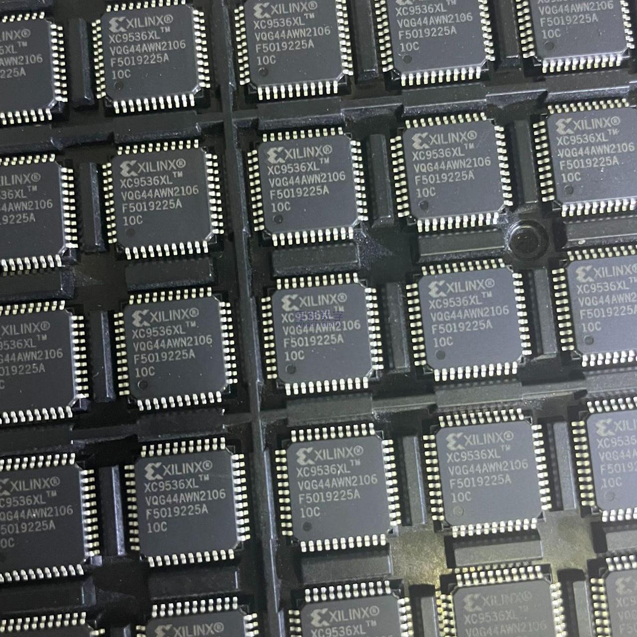
XC9536XL-10VQG44C

XC9500XL CPLD, 36 macrocells, 800 gates, 5ns tPD, 178MHz, 34 I/O, VQFP-44 10x10mm, 3.3V, 5V tolerant, commercial 0-70C, AMD Xilinx

8500

Effective Inventory

Image for reference only

Manufacturer Part:

XC9536XL-10VQG44C

Package:

VQG44 (44-pin very thin quad flat pack, 10x10mm body, 0.8mm lead pitch, 4-sided gull-wing leads, lead-free)

Brand:

Quality Commitment

Shipping & Payment

Service & Packaging

Product Manual

Description

Product Overview

The XC9536XL-10VQG44C is a low-cost, high-performance CPLD from Xilinx (AMD) featuring 36 macrocells in a 44-pin Very Thin Quad Flat Pack (VQFP) package. As the smallest member of the XC9500XL 3.3 V CPLD family, this device provides economical programmable logic for general-purpose logic replacement, bus interfacing, and system control applications.

Built on advanced 0.35 micron CMOS FastFLASH technology, the XC9536XL delivers 5 ns pin-to-pin logic delays with system frequencies up to 178 MHz. The device contains 36 macrocells with approximately 800 usable gates, organized in two 54-input Function Blocks connected by the FastCONNECT II switch matrix. Each macrocell features up to 90 product terms through the intelligent product term allocator, a configurable flip-flop/latch, and independent clock and output enable controls.

The VQG44 package provides 34 user I/O pins in a compact 10 x 10 mm footprint with 0.8 mm lead pitch. I/Os are 5 V tolerant on inputs and support 3.3 V or 2.5 V output levels. Key features include in-system programming via JTAG, individual output slew rate control, input hysteresis, bus-hold circuitry, and hot-plugging support. The -10 speed grade with commercial temperature range (0 degC to 70 degC) is ideal for cost-sensitive consumer and computer applications. 10,000+ program/erase cycle endurance and 20-year data retention ensure long-term reliability.

Key Specifications

Parameter Value
Macrocells 36
Usable Gates 800
Registers 36
Function Blocks 2 (54 inputs each)
Product Terms per Macrocell Up to 90 (via allocator)
Pin-to-Pin Delay (tPD) 5 ns (typical, -10 speed grade)
Setup Time (tSU) 3.7 ns
Clock to Output (tCO) 3.5 ns
System Frequency (fSYSTEM) 178 MHz
Global Clocks 3 (GCK1, GCK2, GCK3)
Global OE Pins 2 (GTS1, GTS2)
Global Set/Reset 1 (GSR)
User I/O Pins (VQ44) 34
Supply Voltage (VCCINT) 3.0 V to 3.6 V (3.3 V nominal)
I/O Supply (VCCIO) 2.5 V or 3.3 V
Input Tolerance 5 V tolerant
Output Standards 3.3 V LVTTL, 2.5 V CMOS
Programming In-System Programming via JTAG (IEEE 1149.1)
Endurance 10,000 program/erase cycles min
Data Retention 20 years minimum
Operating Temperature 0 degC to +70 degC (commercial C-grade)
Package VQG44 / VQFP-44 (10 x 10 mm, 0.8 mm pitch)

Features

  • 36 macrocells, 800 usable gates, 5 ns pin-to-pin delay
  • FastFLASH 0.35 micron CMOS technology
  • High-performance 3.3 V operation
  • 5 V tolerant I/O pins (5V, 3.3V, 2.5V input compatible)
  • 3.3 V or 2.5 V output capability
  • Superior pin-locking with FastCONNECT II switch matrix
  • 54-input Function Blocks for wide logic functions
  • Up to 90 product-terms per macrocell via allocator
  • 3 global clocks + product-term clocks with local inversion
  • Individual output enable per output pin
  • Input hysteresis on all pins (Schmitt trigger)
  • Bus-hold circuitry on all user I/O pins
  • Hot-plugging capability
  • Full IEEE Std 1149.1 JTAG boundary-scan
  • In-system programmable (ISP) via JTAG
  • Fast concurrent programming
  • Slew rate control on individual outputs
  • Enhanced design security features
  • 10,000+ program/erase cycles
  • 20-year data retention
  • Pin-compatible with 5V XC9536 family
  • Compact VQFP-44 package (10 x 10 mm)
  • Lead-free, RoHS compliant

Applications

  • Computer motherboard and peripheral logic
  • Consumer electronics and portable devices
  • Bus interface and level translation
  • Address decoding and glue logic replacement
  • Power supply sequencing and monitoring
  • System configuration and control logic
  • Keyboard and display controllers
  • Quick-turn prototyping and development boards

Product Introduction: XC9536XL-10VQG44C Product Introduction

The XC9536XL-10VQG44C is the smallest member of Xilinx’s XC9500XL CPLD family, offering 36 macrocells in a compact 44-pin Very Thin QFP package. Designed for low-cost, high-performance 3.3V systems, this device is ideal for replacing discrete logic, implementing simple state machines, and providing basic bus interfacing in consumer, computing, and communications applications.

Built on Xilinx’s FastFLASH technology (0.35 micron CMOS), the XC9536XL delivers 5 ns pin-to-pin delays and system frequencies up to 178 MHz – surprisingly fast for a device of this density and cost. The architecture consists of two Function Blocks (FBs), each with 18 macrocells, connected by the FastCONNECT II switch matrix. The FastCONNECT II structure provides fully predictable, uniform routing delays, a key advantage that ensures pin-locked performance: design changes within the same pinout do not affect timing.

Each macrocell has five direct product terms for implementing combinational logic, plus access to the product term allocator which can provide up to 90 product terms per macrocell from other macrocells in the same Function Block. The flip-flop in each macrocell is individually configurable as D, T, JK, or SR type, and can be clocked by any of the three global clocks or by a product-term generated clock. Output enable, set, and reset are also individually configurable.

The VQFP-44 package has a compact 10 x 10 mm footprint with 0.8 mm lead pitch, providing 34 user I/O pins in a form factor well-suited for space-constrained designs. The I/Os are 5V tolerant on the input side, allowing seamless interfacing with legacy 5V logic families, while outputs operate at 3.3V or 2.5V as determined by the VCCIO supply.

In-system programming via the standard JTAG interface enables programming on the board, which is useful for both manufacturing and field upgrades. With 10,000+ program/erase cycles and 20-year data retention, the XC9536XL offers reliability comparable to mask-programmed logic devices while retaining the flexibility of in-system reconfiguration. The XC9536XL is pin-compatible with the 5V XC9536 device, simplifying voltage migration.

Working Principle: XC9536XL-10VQG44C Working Principle

The XC9536XL is a Flash-based Complex Programmable Logic Device. Its architecture and operation are as follows:

1. Function Blocks (FBs): Two Function Blocks, each containing 18 macrocells. Each FB has 54 inputs coming from the FastCONNECT II switch matrix and 18 macrocell outputs feeding back into the switch matrix. The wide 54-input structure allows complex combinatorial functions to be implemented in a single level of logic, contributing to the fast 5 ns pin-to-pin delay.

2. Macrocells: Each macrocell contains:
– An AND array generating five direct product terms
– An OR gate summing the product terms
– A product term allocator that can borrow up to 90 product terms from other macrocells in the same FB for complex logic functions
– A programmable flip-flop (configurable as D, T, JK, SR, or latch, or bypassed for combinatorial output)
– Exclusive-OR gate for output polarity selection (active high or low)
– Output enable multiplexer selecting from global OE, product-term OE, or always enabled
– Individual clock, set, and reset controls

3. FastCONNECT II Switch Matrix: The central routing resource that connects all I/O pins and FB outputs to the FB inputs. Unlike FPGAs where routing delay varies depending on path length, the FastCONNECT matrix provides uniform, predictable delay for all connections. This deterministic timing model is the foundation of the XC9500XL’s pin-locking guarantee – logic changes within a locked pinout do not change timing performance.

4. I/O Blocks (IOBs): Each IOB interfaces between internal logic and the external pin. Key features:
– Input buffer with Schmitt trigger hysteresis for improved noise immunity
– Output driver with programmable slew rate (fast for high-speed, slow for EMI reduction)
– Bus-hold circuit holding unused inputs at their last logic level (eliminates external pull-up/down resistors)
– 5V input tolerance (accepts voltages up to 5.5V even though VCC is 3.3V)
– Output voltage determined by VCCIO (2.5V or 3.3V)
– Hot-plug safe (I/Os do not drive during power-up/down)

5. Global Resources:
– 3 global clock pins (GCK1-3): low-skew distribution to all 36 macrocells
– 2 global output enable pins (GTS1-2): global tri-state control
– 1 global set/reset (GSR): asynchronous initialization of all flip-flops
All global pins are shared with I/O pins and can be used as regular I/O when the global function is not needed.

6. JTAG Boundary Scan and ISP: The JTAG interface provides both IEEE 1149.1 boundary-scan test capability and in-system programming capability. A single 4-pin JTAG port serves both functions. Programming is done concurrently across all macrocells, resulting in very fast programming times. The configuration is stored in non-volatile Flash cells, so the device is “instant-on” at power-up – no external configuration memory needed.

Pin Description: XC9536XL-10VQG44C Pin Definition and Functions
Pin Group Pin Number(s) Type Description
Power VCC (Pin 6, 28) Power Positive supply voltage: 3.3 V nominal (3.0 V to 3.6 V). Two VCC pins. Bypass each with 0.1uF ceramic capacitor to GND.
Power GND (Pin 17, 39) Ground Ground reference pins. Two GND pins. Connect to system ground plane.
User I/O I/O1-I/O34 (various pins) I/O 34 user I/O pins. Each individually configurable as input, output, or bidirectional. 5V tolerant inputs. Output level: 2.5V or 3.3V (set by VCCIO). Individual slew rate control.
Global Clock 1 I/O/GCK1 (Pin 33) Input Global clock input 1. Low skew to all macrocells. Can be used as regular I/O if not needed as clock.
Global Clock 2 I/O/GCK2 (Pin 34) Input Global clock input 2. Shared with I/O. Usable as regular I/O.
Global Clock 3 I/O/GCK3 (Pin 40) Input Global clock input 3. Shared with I/O. Usable as regular I/O.
Global OE 1 I/O/GTS1 (Pin 13) Input Global tri-state/output enable 1. Active low output enable for all I/O pins. Shared with I/O.
Global OE 2 I/O/GTS2 (Pin 14) Input Global tri-state/output enable 2. Shared with I/O. Usable as regular I/O.
Global Set/Reset I/O/GSR (Pin 26) Input Global set/reset input. Asynchronously sets or resets all flip-flops. Shared with I/O.
JTAG TCK TCK (Pin 8) Input JTAG Test Clock input. Dedicated pin. Clock signal for boundary scan test and in-system programming.
JTAG TMS TMS (Pin 7) Input JTAG Test Mode Select. Dedicated pin. Controls the TAP controller state machine.
JTAG TDI TDI (Pin 4) Input JTAG Test Data In. Dedicated pin. Serial data input for boundary scan and programming operations.
JTAG TDO TDO (Pin 38) Output JTAG Test Data Out. Dedicated pin. Serial data output for boundary scan and programming.

Package: VQG44 – 44-pin Very Thin Quad Flat Pack. Body dimensions: 10mm x 10mm x 1.0mm (typical height). Lead pitch: 0.8mm. 11 pins per side (44 total). Gull-wing leads. VQ = Very thin QFP. G = Green / lead-free. Commercial temperature grade: 0 degC to +70 degC ambient. MSL Level 3 (168 hours floor life).

Application Scenarios: In which products and applications is XC9536XL-10VQG44C used
  • Computer Motherboard and Peripheral Logic: Glue logic, address decoding, and simple state machine functions on PC motherboards, graphics cards, storage controllers, and expansion cards. The low cost and small footprint make it ideal for replacing a handful of discrete logic gates in cost-sensitive computer designs.
  • Consumer Electronics: Control logic in consumer devices including set-top boxes, DVD/Blu-ray players, gaming consoles, and home networking equipment. 36 macrocells are sufficient for many system control, I/O expansion, and user interface functions in consumer products.
  • Bus Interface and Level Translation: 5V to 3.3V level shifting and bus interfacing between different voltage domains. The 5V tolerant inputs make the XC9536XL ideal for bridging legacy 5V systems to modern 3.3V designs without external level translators.
  • Address Decoding and Glue Logic Replacement: Replacing PALs, GALs, and multiple discrete logic gates (AND, OR, XOR, flip-flops) with a single CPLD. Reduces component count, PCB area, and BOM cost while adding the flexibility of in-system reprogramming.
  • Power Supply Sequencing and Monitoring: Power-on reset, voltage sequencing, and fault detection circuits for multi-voltage systems including servers, networking equipment, and embedded systems. The instant-on Flash configuration ensures the CPLD is active before other components come up.
  • System Configuration and Control Logic: Board-level control functions including configuration state machines for FPGAs/processors, watchdog timers, and system status monitoring. The 34 I/O pins provide ample connectivity for a typical board management function.
  • Keyboard and Display Controllers: Matrix keyboard scanners, LED display drivers, and simple user interface controllers for appliances, industrial control panels, and consumer devices. The 36 macrocells handle basic scanning and debouncing logic with ease.
  • Quick-Turn Prototyping and Development Boards: FPGA/MCU development boards, evaluation kits, and prototyping platforms where the CPLD serves as a flexible glue-logic and level-shifting element that can be reprogrammed as the design evolves, reducing the need for multiple board spins during development.
Alternative Models: What chips are recommended as replacements for XC9536XL-10VQG44C
Manufacturer Part Number Macrocells I/O tPD Voltage Package Notes
Xilinx XC9536XL-10VQG44I 36 34 5 ns 3.3V VQFP-44 Industrial grade (-40 to +85)
Xilinx XC9536XL-10PCG44C 36 34 5 ns 3.3V PLCC-44 PLCC socket version
Xilinx XC9572XL-10VQG64C 72 52 5 ns 3.3V VQFP-64 Double density, VQFP-64
Lattice LC4032V-75TN44C 32 32 4.5 ns 3.3V TQFP-44 isopMACH 4000V
Intel/Altera EPM7032SLC44-10 32 36 5 ns 3.3V PLCC-44 MAX 7000, 5V tolerant
Microchip/Atmel ATF1502AS-10JC44 32 32 7.5 ns 3.3V PLCC-44 ATF15xx series

Recommend Parts

ISO1176TDWR

Isolated RS-485 transceiver, 40Mbps, integrated transformer driver, SOIC-16

Brand: TI

Package: SOIC-16 (DW, wide-body, 10.3 x 10.3 mm)

IN STOCK: 6874pcs

Cargo cycle: 3-7 Days

The minimum order is 1

IRFB4020PBF

200V N-Channel HEXFET Power MOSFET, 31A, 68 mΩ RDS(on), TO-220AB

Brand: infineon

Package: TO-220AB

IN STOCK: 14149pcs

Cargo cycle: 3-7 Days

The minimum order is 1

NRF52832-QFAA-T

Nordic BLE SoC, ARM Cortex-M4 @ 64MHz, 64KB Flash, 32KB RAM, QFN-48

Package: See datasheet

IN STOCK: 10958pcs

Cargo cycle: 3-7 Days

The minimum order is 1

UCC28740DR

CVCC Flyback Controller, 700V startup, opto feedback, <10mW no-load, SOIC-7

Brand: TI

Package: SOIC-7 (4.9 x 3.9 x 1.75 mm)

IN STOCK: 4840pcs

Cargo cycle: 3-7 Days

The minimum order is 1

MMUN2211LT1G

NPN digital transistor, R1=10kΩ R2=10kΩ, 50V, 100mA, SOT-23-3, pre-biased BRT switch

Brand: Onsemi

Package: SOT-23-3 (TO-236, SC-59)

IN STOCK: 8500pcs

Cargo cycle: 3-7 Days

The minimum order is 1

TMS320F2810PBKA

C2000 Delfino DSP controller, 150MHz, 128KB Flash, BGA-179

Brand: TI

Package: BGA-179 (16 x 16 mm, PBK package)

IN STOCK: 3124pcs

Cargo cycle: 3-7 Days

The minimum order is 1




