






Opens in a new tab

Home » Battery Management ICs, LED Driver ICs » XMC4700F144K2048AAXQ

XMC4700F144K2048AAXQ

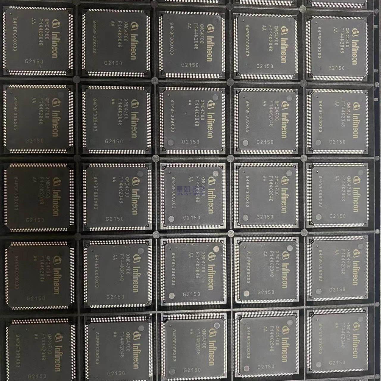
XMC4000 32-bit MCU, ARM Cortex-M4F 144MHz, 2MB Flash, 352KB SRAM, 58ch 12bit ADC, Ethernet+USB+CAN, LQFP-144, Infineon, industrial motor control

1200

Effective Inventory

Image for reference only

Manufacturer Part:

XMC4700F144K2048AAXQ

Package:

LQFP-144 (144-pin low-profile quad flat pack, 20x20mm body, 0.5mm lead pitch, 4-sided gull-wing leads)

Brand:

Quality Commitment

Shipping & Payment

Service & Packaging

Product Manual

Description

Product Overview

The XMC4700F144K2048AAXQ is a high-performance 32-bit microcontroller from Infineon Technologies, based on the ARM Cortex-M4F core with DSP instruction set and floating-point unit (FPU). Part of the XMC4000 family optimized for industrial applications, this device operates at up to 144 MHz and features 2 MB of embedded Flash memory, 352 KB of SRAM, and a rich set of peripherals including motor control, communication, and analog interfaces.

Built on Infineon’s proven 65 nm embedded Flash technology, the XMC4700 delivers 144 MHz CPU operation with 1.25 DMIPS/MHz performance. The Cortex-M4F core provides single-cycle multiply-accumulate operations, hardware division, and single-precision floating-point support, making it well-suited for motor control, digital power conversion, and DSP-intensive industrial applications.

Housed in a 144-pin LQFP package (20 x 20 mm, 0.5 mm pitch), the XMC4700 provides up to 112 general-purpose I/O pins. Key peripherals include four 12-bit ADC modules with up to 58 channels and 300 ns conversion time, two 12-bit DACs, 16 general-purpose timers (CCU4/CCU8), four 16-channel capture/compare units for motor control, a Position Interface (POSIF) for encoder support, Ethernet MAC, USB 2.0 FS OTG, multiple CAN nodes, and several serial communication interfaces (USIC, SPI, I2C, I2S). The device operates from 3.3 V supply over the -40 degC to +85 degC industrial temperature range.

Key Specifications

Parameter Value
Core ARM Cortex-M4F (32-bit, DSP + FPU)
Max CPU Frequency 144 MHz
Performance 1.25 DMIPS / MHz (180 DMIPS)
Flash Memory 2,048 KB (2 MB) embedded Flash
SRAM 352 KB total (PSRAM + DSRAM + USIC0/1/2 RAM)
Cache 8 KB instruction cache
ADC 4 x 12-bit ADCs (VADC), up to 58 channels, 300 ns conversion
DAC 2 x 12-bit DACs
Comparator 4 x analog comparators (ACMP)
Timer Modules CCU4 (4 timers/ch), CCU8 (4 timers/ch), CCU40/41/42/43, CCU80/81
PWM Channels Up to 64 (CCU4) + 24 (CCU8) = 88 PWM outputs
Position Interface POSIF (quadrature encoder, hall sensor, multi-channel pattern)
Ethernet 10/100 Mbps Ethernet MAC (IEEE 1588 PTP support)
USB USB 2.0 Full-Speed OTG (Host + Device)
CAN MultiCAN+ (up to 3 nodes, 256 message objects)
Serial Interfaces 6 USIC channels (UART/SPI/I2C/I2S/SSC)
I2C Via USIC channels
GPIO Up to 112 I/O pins
SD/MMC SDIO / MMC interface
External Memory EBU (External Bus Unit) for SDRAM/NOR/NAND
Operating Voltage 3.3 V (2.97 V to 3.63 V)
Core Voltage 1.3 V (internal regulator)
Operating Temperature -40 degC to +85 degC (industrial)
Package LQFP-144 (20 x 20 mm, 0.5 mm pitch)
Process Technology 65 nm embedded Flash

Features

  • ARM Cortex-M4F core with DSP and FPU, up to 144 MHz
  • 2 MB high-density embedded Flash (65nm technology)
  • 352 KB total SRAM (including USB/CAN/I2C dedicated RAM)
  • 8 KB instruction cache for faster code execution
  • Memory Protection Unit (MPU)
  • Nested Vectored Interrupt Controller (NVIC): 124 channels
  • 4 x 12-bit ADC modules (VADC), up to 58 channels, 300 ns conversion
  • 2 x 12-bit DACs with flexible trigger options
  • 4 x analog comparators with programmable references
  • CCU4: 4 capture/compare timer units (4 channels each = 16 total)
  • CCU8: 2 capture/compare timer units (8 channels each = 16 total)
  • POSIF: position interface for quadrature encoder and hall sensors
  • 10/100 Mbps Ethernet MAC with IEEE 1588 PTP
  • USB 2.0 Full-Speed OTG (Host + Device)
  • MultiCAN+ with up to 3 nodes and 256 message objects
  • 6 Universal Serial Interface Channels (USIC): UART, SPI, I2C, I2S, SSC
  • SD/MMC interface (SDIO 4-bit, up to 48 MHz)
  • External Bus Unit (EBU) for SDR-SDRAM, NOR, NAND Flash
  • Real-time clock (RTC) with alarm function
  • Window watchdog and backup watchdog timers
  • Up to 112 general-purpose I/O pins
  • Internal 1.3 V core voltage regulator
  • Power-on reset and brown-out detection
  • Integrated temperature sensor
  • 16-bit CRC unit for flash memory integrity check
  • Flash ECC (error correction code)
  • JTAG and SWD debug interfaces
  • CoreSight ETB (Embedded Trace Buffer)
  • Dave 4 development tools (IDE + peripheral libraries)
  • Industrial temperature range: -40 degC to +85 degC
  • LQFP-144 package, RoHS compliant

Applications

  • Industrial motor control and drives
  • Power conversion and renewable energy
  • Factory automation and PLC systems
  • Building automation and HVAC control
  • Renewable energy inverters (solar, wind)
  • Uninterruptible power supplies (UPS)
  • Automotive charging and EV systems
  • Communication gateways and IoT edge nodes

Product Introduction: XMC4700F144K2048AAXQ Product Introduction

The XMC4700F144K2048AAXQ is a high-performance 32-bit microcontroller from Infineon’s XMC4000 family, designed specifically for industrial applications including motor control, power conversion, and factory automation. Based on the ARM Cortex-M4F CPU core with DSP extensions and a hardware floating-point unit, this device operates at up to 144 MHz, delivering 180 DMIPS of processing performance.

Manufactured on Infineon’s 65nm embedded Flash technology, the XMC4700 integrates 2 MB of program Flash memory and 352 KB of SRAM. An 8 KB instruction cache accelerates code execution from Flash by reducing wait states. The Cortex-M4F core provides single-cycle multiply-accumulate (MAC) operations, hardware division, saturated arithmetic (DSP extensions), and single-precision floating-point (FPU), making it highly efficient for motor control algorithms and digital power conversion calculations.

Peripheral integration is extensive and optimized for industrial control. Four 12-bit VADC modules provide up to 58 analog input channels with 300 ns conversion time and flexible trigger mechanisms. Two 12-bit DACs and four analog comparators round out the analog capability. For motor control and power conversion, CCU4 and CCU8 timer units provide up to 88 PWM outputs with dead-time generation, plus a POSIF module for quadrature encoder and Hall sensor interface.

Communication peripherals include a 10/100 Mbps Ethernet MAC with IEEE 1588 PTP support, USB 2.0 Full-Speed OTG, MultiCAN+ with up to 3 nodes, and six Universal Serial Interface Channels (USIC) configurable as UART, SPI, I2C, I2S, or SSC. An External Bus Unit (EBU) supports expansion with SDRAM, NOR Flash, or NAND Flash.

The LQFP-144 package provides up to 112 general-purpose I/O pins in a 20 x 20 mm footprint with 0.5 mm lead pitch. The device operates from a single 3.3 V supply (with integrated core regulator) over the -40 degC to +85 degC industrial temperature range. Infineon’s DAVE 4 development environment provides a free Eclipse-based IDE with comprehensive peripheral libraries and code generation tools.

Working Principle: XMC4700F144K2048AAXQ Working Principle

The XMC4700 is a complex 32-bit microcontroller built around the ARM Cortex-M4F core with extensive industrial peripherals. Here are the key subsystems:

1. ARM Cortex-M4F Core: The central processing unit is an ARM Cortex-M4F 32-bit RISC core with the following features:
– Thumb-2 instruction set (16/32-bit mixed instruction encoding for high code density)
– DSP extensions: single-cycle 32×32 MAC, SIMD arithmetic, saturated math
– Single-precision floating-point unit (FPU): IEEE 754-compliant
– Nested Vectored Interrupt Controller (NVIC) with 124 interrupt channels, configurable priorities
– Memory Protection Unit (MPU) for task isolation
– System tick timer, Bit-Band addressing, Wake-up Interrupt Controller
– CoreSight debug + Embedded Trace Buffer (ETB) for code trace

2. Memory Architecture:
– Program Flash: 2 MB embedded Flash (65nm technology), single-cycle access via prefetch buffer + 8KB instruction cache. ECC (Error Correcting Code) for reliability.
– Data Flash: ~64KB Flash dedicated for data storage (emulated EEPROM)
– SRAM: 352 KB total SRAM, organized into multiple blocks (PSRAM for program/data, DSRAM for DMA, plus dedicated RAM for USB, CAN, I2C peripherals)
– External Bus Unit (EBU): supports SDR-SDRAM (up to 64MB), NOR Flash (up to 4 banks), and NAND Flash (with ECC)

3. VADC (Versatile Analog-to-Digital Converter): Four independent ADC modules, each with 12-bit resolution and up to ~14 channels. Features include 300 ns conversion time, auto-scan, queued request sources, result FIFO, limit checking, and flexible trigger gating from timer units. Enables simultaneous sampling of multiple motor phase currents and voltages.

4. CCU4 / CCU8 Timer Units:
– CCU4: 4 modules with 4 capture/compare channels each (16 channels total). Each channel has a 16-bit timer, compare register, and capture register. Used for general-purpose timing, PWM generation, and input capture.
– CCU8: 2 modules with 8 channels each (16 channels total). Each slice has a 16-bit timer with dead-time generation, asymmetric PWM support, and multi-channel pattern generation. Optimized for 3-phase motor control and power conversion.

5. POSIF (Position Interface): A dedicated position sensor interface supporting:
– Quadrature encoder (ABZ) interface with position counter
– Hall sensor interface with pattern matching
– Multi-channel pattern switch for BLDC motor commutation
Works closely with CCU8 for motor control applications.

6. Communication Peripherals:
– Ethernet MAC: 10/100 Mbps with IEEE 1588 PTP hardware timestamping, DMA support, RMII/MII PHY interface
– USB 2.0 FS OTG: Host and device mode with integrated transceiver
– MultiCAN+: 3 CAN nodes with 256 message objects, 64 receive objects with FIFO
– USIC: 6 universal serial interface channels, each configurable as UART, SPI, I2C, I2S, or SSC
– SDIO: SD/MMC card interface (4-bit mode, up to 48 MHz)

7. Power Management and System Control: An on-chip voltage regulator generates the 1.3V core supply from the 3.3V I/O supply. Power-on reset and brown-out detection ensure proper startup and supply monitoring. Multiple low-power modes (Sleep, Deep Sleep, Hibernate) reduce power consumption when full performance is not needed.

Pin Description: XMC4700F144K2048AAXQ Pin Definition and Functions

r>

Pin Group Pin Name(s) Type Description
Power VDD (3.3V) Power I/O and pre-regulator supply: 3.3 V nominal (2.97 V to 3.63 V). Multiple VDD pins distributed around package. All must be connected with decoupling caps.
Power VDDC (1.3V) Power Core logic supply: 1.3 V (generated by internal regulator). Connect external bypass capacitors. Do not power externally unless using external regulator mode.
Power VDDA / VREF+ Power Analog supply for ADC/DAC and reference. Nominally 3.3V (same as VDD). Connect to filtered analog supply for best ADC performance. VREF+ is the positive reference for ADC.
Power VSS / VSSA Ground Digital ground (VSS) and analog ground (VSSA). Multiple ground pins. VSSA should connect to quiet analog ground plane.
Power VBAT Power RTC backup supply: 1.8 V to 3.6 V. Powers RTC, backup registers, and SRAM when VDD is removed. Connect to battery or supercap.
Oscillator XTAL1, XTAL2 I/O Main crystal oscillator: 4 MHz to 25 MHz external crystal. Or single-ended external clock on XTAL1. Primary clock source for system.
RTC Crystal XTAL32K1, XTAL32K2 I/O 32.768 kHz crystal oscillator for real-time clock (RTC). Connect 32.768 kHz watch crystal with load capacitors.
Reset /RST Input Active-low reset input. Schmitt trigger input with internal pull-up. Connect to reset generator/button.
Boot Mode BOOT0, BOOT1 Input Boot configuration pins. Determine boot source at reset (Flash, ROM bootloader, etc.). Sampled during reset sequence.
Debug SWD_CLK, SWD_IO I/O Serial Wire Debug interface: clock and data. Standard ARM debug interface. JTAG also available via other pins.
Debug JTAG (TCK/TMS/TDI/TDO/TRST) I/O JTAG debug interface pins (alternate to SWD). Used for boundary scan and full JTAG debug.
Ethernet ETH_RX_CLK, ETH_RXD0-3, ETH_RX_DV, ETH_RX_ER, ETH_TX_CLK, ETH_TXD0-3, ETH_TX_EN, ETH_TX_ER, ETH_MDC, ETH_MDIO, ETH_REF_CLK I/O Ethernet MAC interface pins (MII or RMII mode). Connect to external Ethernet PHY transceiver.
USB USB_DP, USB_DM, USB_VBUS, USB_ID I/O USB 2.0 Full-Speed OTG differential data pins, VBUS sense, and ID pin for OTG role detection.
CAN CAN_RD, CAN_TD I/O CAN receive and transmit data lines. Connect to external CAN transceiver. Multiple CAN nodes available via pin remapping.
ADC AN0-AN57 (VADC inputs) Analog Input Up to 58 analog input channels for the 12-bit VADC modules. Shared with GPIO pins.
GPIO P0-P9 (ports) I/O Up to 112 general-purpose I/O pins across ports P0 through P9. Configurable as input, output, open-drain, alternate function (peripheral).
PWM/Timer CC40/41/42/43, CC80/81 outputs Output Timer PWM output pins from CCU4 and CCU8 units. Used for motor control PWM, general-purpose PWM, and capture inputs.

Package: LQFP-144 – Low-profile Quad Flat Pack, 144 pins. Body dimensions: 20mm x 20mm. Lead pitch: 0.5mm. 36 pins per side (4 sides). Gull-wing leads. LQFP = Low-profile QFP. XQ suffix denotes industrial temperature grade and specific ordering variant. Operating temperature: -40 degC to +85 degC.

Application Scenarios: In which products and applications is XMC4700F144K2048AAXQ used
  • Industrial Motor Control and Drives: AC induction motor drives, BLDC/PMSM servo drives, and variable frequency drives (VFDs) where the Cortex-M4F DSP + FPU executes field-oriented control (FOC) algorithms, CCU4/CCU8 timers generate high-resolution PWM with dead-time compensation, VADC provides simultaneous current/voltage sampling, and POSIF interfaces with position encoders and Hall sensors.
  • Power Conversion and Renewable Energy: Solar inverters, wind turbine converters, battery management systems (BMS), and DC-DC converters requiring high-performance control loops, analog measurement, and flexible PWM generation. FPU-enabled control loops with floating-point math improve control accuracy and simplify firmware development.
  • Factory Automation and PLC: PLC CPUs, remote I/O controllers, and industrial Ethernet gateways (PROFINET, EtherCAT, Modbus TCP) where the Ethernet MAC with IEEE 1588 PTP supports real-time industrial communication, MultiCAN+ provides CAN bus connectivity, and ample Flash/SRAM support complex control programs and communication stacks.
  • Building Automation and HVAC: HVAC controllers, building management systems (BMS), and smart building gateways requiring multiple communication interfaces (Ethernet, CAN, RS-485, USB), analog I/O for environmental sensors, and sufficient processing power for building automation protocols and algorithms.
  • Uninterruptible Power Supplies (UPS): Digital control of online and line-interactive UPS systems, including inverter control, battery charging management, and static switch control. High-resolution PWM, fast ADC sampling, and DSP control loops ensure high efficiency and tight output regulation.
  • EV Charging and Automotive Power Electronics: On-board chargers (OBC), DC-DC converters, and charging infrastructure for electric vehicles requiring high-power digital control with efficient PWM generation, isolated sensing interfaces, and communication (CAN, Ethernet, PLC). Industrial temperature range and robust Flash technology suit automotive applications.
  • Communication Gateways and IoT Edge Nodes: Industrial IoT edge gateways and protocol converters bridging between multiple industrial networks (EtherNet/IP, PROFINET, CAN, RS-485). The combination of Ethernet MAC, CAN, multiple serial ports, and 2MB Flash enables running full protocol stacks and application logic simultaneously.
  • Digital Power Supplies and Lighting: High-efficiency digital power supplies, smart LED drivers, and power management units requiring advanced control algorithms (e.g., resonant LLC control, PFC), multiple PWM channels, and fast analog feedback loops. The Cortex-M4F with DSP extensions handles complex control schemes that analog controllers cannot implement.
Alternative Models: What chips are recommended as replacements for XMC4700F144K2048AAXQ
Manufacturer Part Number Core Flash RAM Package Notes
Infineon XMC4800F144K2048AA Cortex-M4F 144MHz 2 MB 352 KB LQFP-144 Same family, adds EtherCAT
Infineon XMC4700F144K2048BAXQ Cortex-M4F 144MHz 2 MB 352 KB BGA-196 BGA package variant
Infineon XMC4500F144K1024AC Cortex-M4F 120MHz 1 MB 160 KB LQFP-144 Lower cost variant
STMicro STM32F427ZGT6 Cortex-M4F 180MHz 1 MB 256 KB LQFP-144 STM32F4, higher freq
NXP LPC54628J512ET180 Cortex-M4F 220MHz 512 KB 200 KB LQFP-180 LPC54000, higher speed
TI TMS320F28379D C28x + CLA 200MHz 1 MB 204 KB LQFP-176 C2000 Delfino, DSP focus

Recommend Parts

ISO1176TDWR

Isolated RS-485 transceiver, 40Mbps, integrated transformer driver, SOIC-16

Brand: TI

Package: SOIC-16 (DW, wide-body, 10.3 x 10.3 mm)

IN STOCK: 6874pcs

Cargo cycle: 3-7 Days

The minimum order is 1

IRFB4020PBF

200V N-Channel HEXFET Power MOSFET, 31A, 68 mΩ RDS(on), TO-220AB

Brand: infineon

Package: TO-220AB

IN STOCK: 14149pcs

Cargo cycle: 3-7 Days

The minimum order is 1

NRF52832-QFAA-T

Nordic BLE SoC, ARM Cortex-M4 @ 64MHz, 64KB Flash, 32KB RAM, QFN-48

Package: See datasheet

IN STOCK: 10958pcs

Cargo cycle: 3-7 Days

The minimum order is 1

UCC28740DR

CVCC Flyback Controller, 700V startup, opto feedback, <10mW no-load, SOIC-7

Brand: TI

Package: SOIC-7 (4.9 x 3.9 x 1.75 mm)

IN STOCK: 4840pcs

Cargo cycle: 3-7 Days

The minimum order is 1

MMUN2211LT1G

NPN digital transistor, R1=10kΩ R2=10kΩ, 50V, 100mA, SOT-23-3, pre-biased BRT switch

Brand: Onsemi

Package: SOT-23-3 (TO-236, SC-59)

IN STOCK: 8500pcs

Cargo cycle: 3-7 Days

The minimum order is 1

TMS320F2810PBKA

C2000 Delfino DSP controller, 150MHz, 128KB Flash, BGA-179

Brand: TI

Package: BGA-179 (16 x 16 mm, PBK package)

IN STOCK: 3124pcs

Cargo cycle: 3-7 Days

The minimum order is 1




