





Opens in a new tab

STM32F103C8T6

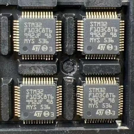
STM32 ARM Cortex-M3 MCU, 72MHz, 64KB Flash, 20KB SRAM, 10ch 12bit ADC, USB+CAN+SPI+I2C+USART, LQFP-48, STMicroelectronics, medium-density

6800

Effective Inventory

Image for reference only

Manufacturer Part:

STM32F103C8T6

Package:

LQFP-48 (48-pin low-profile quad flat pack, 7x7mm body, 0.5mm lead pitch, 12 pins per side, gull-wing leads)

Quality Commitment

Shipping & Payment

Service & Packaging

Product Manual

Description

Product Overview

The STM32F103C8T6 is a 32-bit microcontroller from STMicroelectronics based on the ARM Cortex-M3 RISC core operating at 72 MHz frequency. It belongs to the STM32F103 medium-density performance line family, offering high integration and cost-effectiveness for a wide range of embedded applications.

Built on the ARM Cortex-M3 core with 72 MHz operating frequency, the STM32F103C8T6 features 64 KB of embedded Flash memory and 20 KB of SRAM. The Cortex-M3 core provides Thumb-2 instruction set, hardware division, bit-banding, and nested vectored interrupt controller (NVIC) with 43 maskable interrupt channels and 16 priority levels. The device includes a comprehensive set of peripherals: two 12-bit ADCs with up to 10 input channels, up to 37 fast I/O ports, three general-purpose 16-bit timers, one advanced-control PWM timer, an I2C interface, two SPI interfaces, two USARTs, a USB 2.0 full-speed interface, and a CAN interface.

Housed in a 48-pin LQFP package with 7 x 7 mm footprint and 0.5 mm lead pitch, the STM32F103C8T6 operates from 2.0 V to 3.6 V supply voltage over the -40 °C to +85 °C industrial temperature range. Its extensive peripheral set, high CPU performance, and low cost make it one of the most popular and widely used microcontrollers in the embedded industry, particularly in hobbyist, industrial, and consumer electronics applications.

Key Specifications

Parameter Value
Core ARM Cortex-M3 (32-bit RISC)
Max CPU Frequency 72 MHz
Performance 1.25 DMIPS/MHz (90 DMIPS)
Flash Memory 64 KB
SRAM 20 KB
ADC 2 x 12-bit ADC, up to 10 channels, 1 µs conversion
DAC None (no DAC in medium-density F103)
Advanced Timer (TIM1) 1 (16-bit, 6-channel PWM, 8-channel DMA)
General-Purpose Timers 3 (TIM2/TIM3/TIM4, 16-bit, each 4 channels)
Watchdog Timers Independent WDT + Window WDT
SPI 2 (up to 18 Mbit/s)
I2C 2 (up to 400 kHz, Fast Mode)
USART 3 (up to 4.5 Mbit/s)
USB USB 2.0 Full-Speed Device (12 Mbit/s)
CAN CAN 2.0A/B (1 Mbit/s)
DMA Controller 7 channels (DMA1)
GPIO 37 fast I/O ports (5 V tolerant, up to 50 MHz)
Operating Voltage 2.0 V to 3.6 V
Low-Power Modes Sleep, Stop, Standby
RTC Real-time clock with 32 kHz external crystal
Operating Temperature -40 °C to +85 °C (industrial)
Package LQFP-48 (7 x 7 mm, 0.5 mm pitch)
Debug Interface SWD (Serial Wire Debug) + JTAG

Features

  • ARM Cortex-M3 32-bit core @ 72 MHz
  • 64 KB Flash memory with protection
  • 20 KB SRAM (zero wait state @ 72 MHz)
  • Nested Vectored Interrupt Controller (NVIC)
  • 2 x 12-bit ADC (1 µs conversion, up to 10 external channels)
  • Temperature sensor (internal ADC channel)
  • Advanced-control timer TIM1 (16-bit, up to 6 PWM outputs)
  • 3 general-purpose timers (TIM2/3/4, each 4 channels)
  • Independent and window watchdog timers
  • SysTick timer (24-bit down counter)
  • 2 SPI interfaces (up to 18 Mbit/s)
  • 2 I2C interfaces (SMBus/PMBus compatible)
  • 3 USARTs (ISO 7816, LIN, IrDA, modem control)
  • USB 2.0 Full-Speed Device interface
  • CAN 2.0A/B (1 Mbit/s)
  • 7-channel DMA controller
  • Up to 37 fast I/O pins, 5 V tolerant
  • Real-time clock (RTC) with 32.768 kHz oscillator
  • Internal 8 MHz RC oscillator + 40 kHz RC for watchdog
  • PLL for CPU clock multiplication
  • Low-power modes: Sleep, Stop, Standby
  • Power-on reset / power-down reset / brown-out reset
  • Serial Wire Debug (SWD) + JTAG
  • Flash memory read protection
  • 2.0 V to 3.6 V operating supply
  • LQFP-48 package, 7 x 7 mm
  • Industrial temperature range: -40 to +85 °C

Applications

  • Industrial control and automation
  • Consumer electronics and home appliances
  • IoT and connected devices
  • Motor control and power conversion
  • Medical and healthcare devices
  • Wearable and fitness trackers
  • Robotics and drones
  • Education and development boards (Blue Pill, etc.)

Product Introduction: STM32F103C8T6 Product Introduction

The STM32F103C8T6 is a medium-density member of the STM32F1 series performance line from STMicroelectronics, built around the ARM Cortex-M3 32-bit RISC core operating at 72 MHz. This device is one of the most popular and widely used microcontrollers in the embedded industry, valued for its excellent price-performance ratio and extensive peripheral integration.

The Cortex-M3 core delivers 1.25 DMIPS per MHz for a total of 90 DMIPS at 72 MHz. It features the Thumb-2 instruction set for high code density, hardware single-cycle 32×32 multiply and 32-bit division, bit-banding for atomic bit manipulation, and a Nested Vectored Interrupt Controller (NVIC) with 43 maskable interrupt channels and 16 priority levels. The built-in SysTick timer provides a simple system tick for RTOS operation.

Memory resources include 64 KB of embedded Flash with read protection capability and 20 KB of static RAM with zero-wait-state access at 72 MHz. The Flash can be programmed via the SWD/JTAG interface or through the system bootloader (USART or USB DFU).

The peripheral set is exceptionally rich for a device of this cost level. Two 12-bit ADCs provide up to 10 external input channels with 1 µs conversion time and internal temperature sensor. Four timers (one advanced-control TIM1 + three general-purpose TIM2/3/4) support PWM generation, input capture, output compare, and encoder interfaces. Communication peripherals include two SPI interfaces, two I2C interfaces, three USARTs, USB 2.0 Full-Speed Device, and CAN 2.0B – making it suitable for a vast range of connectivity applications.

The LQFP-48 package provides 37 general-purpose I/O pins in a compact 7×7 mm footprint. Most I/O pins are 5 V tolerant and can toggle at speeds up to 50 MHz. The device operates from 2.0 V to 3.6 V supply, with an internal voltage regulator providing the 1.8 V core supply. Low-power modes (Sleep, Stop, Standby) enable power-efficient operation in battery-powered applications.

Working Principle: STM32F103C8T6 Working Principle

The STM32F103C8T6 is a complex system-on-chip built around the ARM Cortex-M3 core. Here are the key subsystems:

1. ARM Cortex-M3 Core: The central processing unit is the ARM Cortex-M3 32-bit RISC processor with:
– 3-stage pipeline (fetch, decode, execute) with branch prediction
– Thumb-2 instruction set (mix of 16-bit and 32-bit instructions for high code density)
– Hardware multiply (single-cycle 32×32) and divide (2-12 cycles)
– Bit-banding for atomic bit-level access (bit-banding maps each bit to a full 32-bit word in alias region)
– Nested Vectored Interrupt Controller (NVIC) with 43 channels, 16 priority levels, tail-chaining
– SysTick 24-bit system tick timer (typically 1ms for RTOS)
– Memory Protection Unit (MPU) – available on connectivity line but basic on F103
– CoreSight debug with SWD (Serial Wire Debug) and JTAG interfaces

2. Memory Architecture:
– Flash Memory: 64 KB on-chip Flash (starts at address 0x08000000). Zero wait-state up to 24 MHz; prefetch buffer for 72 MHz operation. Supports in-system programming (ISP) and in-application programming (IAP). Read-out protection (RDP) prevents code reverse-engineering.
– SRAM: 20 KB static RAM (starts at 0x20000000). Zero wait-state at full 72 MHz speed. Data is retained in Stop and Standby modes (with backup power).
– Bit-Band: Both SRAM and peripheral registers support bit-banding – a 1 MB alias region maps each bit to a full 32-bit word, enabling atomic bit set/clear without read-modify-write.
– System Boot ROM: 2 KB internal boot ROM (at 0x1FFFF000) with bootloader supporting USART and USB DFU programming.

3. Clock System:
– Internal 8 MHz RC oscillator (HSI) – 1% accuracy at 25C
– External high-speed oscillator (HSE) – 4-16 MHz crystal (typically 8 MHz)
– PLL: multiplies HSI/HSE up to 72 MHz (max CPU clock)
– Internal 40 kHz RC for IWDG (independent watchdog)
– External 32.768 kHz crystal (LSE) for RTC
– Internal 30-60 kHz RC (LSI) for RTC backup and WWDG

4. Peripheral Subsystem:
– ADC: Two 12-bit successive approximation ADCs (1 µs conversion). Shared analog channels. Supports simultaneous sampling, scan mode, DMA transfer. Internal temperature sensor and internal reference voltage channels.
– Timers: TIM1 (advanced-control, 16-bit, 6 PWM channels with dead-time insertion), TIM2/3/4 (general-purpose, 16-bit, each with 4 capture/compare channels). Support PWM, input capture, output compare, one-pulse mode, encoder interface.
– Communication: SPI (2 units, up to 18 Mbit/s, master/slave), I2C (2 units, 100/400 kHz, SMBus compatible), USART (3 units, 4.5 Mbit/s, with flow control), USB 2.0 FS Device (12 Mbit/s, 8 endpoints), CAN 2.0B (1 Mbit/s, 14 filters).
– DMA: 1 DMA controller with 7 channels, supporting memory-to-memory, peripheral-to-memory, and memory-to-peripheral transfers. Circular and normal modes.
– GPIO: 37 I/O pins organized into ports A, B, C. Configurable as input (floating/pull-up/pull-down/analog), output (push-pull/open-drain), alternate function, or analog. 5 V tolerant on most pins. Speed selectable (2/10/50 MHz).

5. Power Management:
– Internal voltage regulator generates 1.8 V core supply from VDD (2.0-3.6 V)
– Sleep mode: CPU stopped, all peripherals active
– Stop mode: All clocks stopped, SRAM and registers retained
– Standby mode: Only RTC, backup registers, and 4 KB SRAM retained
– POR/PDR/BOR: Power-on reset, power-down reset, brown-out reset

Pin Description: STM32F103C8T6 Pin Definition and Functions

r>

Pin Group Pin Names Type Description
Power VBAT Power RTC backup power supply: 1.8 V to 3.6 V. Powers RTC, backup registers, and 4 KB backup SRAM when VDD is off. Connect to battery or supercap.
Power VDD (Pin 5, 17, 30, 43, 47) Power Main I/O and pre-regulator supply: 2.0 V to 3.6 V. Multiple VDD pins. All must be connected with 100nF decoupling caps. VDD = 2.0-3.6 V (typical 3.3 V).
Power VSS (Pin 4, 16, 29, 42, 46) Ground Ground / VSS. Multiple ground pins. Connect to ground plane.
Power VDDA (Pin 9) Power Analog supply for ADC: same as VDD (2.4 V to 3.6 V). Connect to filtered analog supply for best ADC performance. Ferrite bead or filter from VDD recommended.
Power VSSA (Pin 8) Ground Analog ground. Connect to analog ground plane.
Oscillator OSC_IN (PD0, Pin 5) Input High-speed external oscillator input. Connect 4-16 MHz crystal (typically 8 MHz). Can also be used as GPIO PD0.
Oscillator OSC_OUT (PD1, Pin 6) Output High-speed external oscillator output. Connect to other side of crystal. Can also be GPIO PD1.
RTC OSC32_IN (PC14, Pin 2) Input 32.768 kHz low-speed external crystal input for RTC. Can also be GPIO PC14.
RTC OSC32_OUT (PC15, Pin 3) Output 32.768 kHz low-speed external crystal output. Can also be GPIO PC15.
Reset NRST (Pin 7) I/O Active-low reset pin. Bidirectional: external reset input, internal reset output. Schmitt trigger with pull-up. Connect to reset circuit (RC or reset IC).
Boot BOOT0 (Pin 44) Input Boot mode selection. BOOT0=0: boot from Flash (normal). BOOT0=1: boot from system memory (bootloader). Pulled low by default.
Debug SWDIO (PA13, Pin 34) I/O Serial Wire Debug data I/O. Also JTAG TMS. Must be connected for SWD/JTAG programming and debug.
Debug SWCLK (PA14, Pin 37) Input Serial Wire Debug clock. Also JTAG TCK. Required for SWD/JTAG debug interface.
USB PA12 (USB_DP), PA11 (USB_DM) I/O USB 2.0 Full-Speed differential data pins. Connect to USB connector. PA12 = D+, PA11 = D-.
CAN PA11 (CAN_RX), PA12 (CAN_TX) I/O CAN bus receive and transmit pins. Shared with USB (alternate function). Connect to CAN transceiver.
ADC PA0-PA7, PB0, PB1 (10 channels) Analog Input ADC analog input channels. PA0-PA7 = ADC_CH0-CH7, PB0 = ADC_CH8, PB1 = ADC_CH9. Shared with GPIO.
GPIO PA0-PA15, PB0-PB15, PC13-PC15 I/O General-purpose I/O ports. Port A (16 pins), Port B (16 pins), Port C (3 pins: PC13/14/15). Total 37 usable I/O pins. 5V tolerant except analog pins.
Timer PWM TIM1_CH1-CH4, TIM2_CH1-CH4, etc. I/O Timer capture/compare and PWM output pins from TIM1, TIM2, TIM3, TIM4. Shared with GPIO pins via alternate function.

Package: LQFP-48 – Low-profile Quad Flat Pack, 48 pins. Body: 7mm x 7mm. Lead pitch: 0.5mm. 12 pins per side. Gull-wing leads. Exposed pad. -C in part number denotes 48-pin package. -T6 suffix denotes LQFP package. Operating temperature: -40 °C to +85 °C (industrial grade).

Application Scenarios: In which products and applications is STM32F103C8T6 used
  • Industrial Control and Automation: PLC I/O modules, sensor interfaces, small PLC CPUs, motor controllers, and factory automation equipment where the combination of multiple communication interfaces (CAN, USART, SPI, I2C), PWM timers, and ADCs enables complete control system integration in a single low-cost chip.
  • Consumer Electronics and Home Appliances: Smart home devices, kitchen appliances, air conditioners, and consumer IoT products requiring wireless connectivity (via SPI/I2C to radio modules), user interfaces, and application control logic. The USB interface enables easy firmware updates and device configuration.
  • IoT and Connected Devices: IoT sensor nodes, smart meters, environmental monitors, and connected industrial devices where the low cost, multiple communication interfaces, and low-power modes enable battery-operated wireless sensor nodes with cloud connectivity via Wi-Fi/Bluetooth modules.
  • Motor Control and Power Conversion: BLDC motor drives, stepper motor controllers, DC-DC converters, and battery chargers where the advanced timer (TIM1) with complementary PWM outputs and dead-time insertion, fast ADC for current/voltage sampling, and CAN interface provide everything needed for a complete digital motor controller.
  • Medical and Healthcare Devices: Patient monitors, infusion pumps, diagnostic equipment, and medical sensors requiring precise analog measurement, low-power operation, and USB connectivity for data transfer. The Cortex-M3 core provides sufficient processing for signal conditioning and control algorithms.
  • Wearable and Fitness Trackers: Low-cost fitness bands, activity trackers, and health monitors where the STM32F103’s low-power modes, small package, and rich peripheral set enable compact designs with sensor interfaces (I2C/SPI to accelerometers, heart rate sensors) and USB charging/data.
  • Robotics and Drones: Flight controllers, motor ESCs (electronic speed controllers), robot joint controllers, and robotic arm controllers where multiple PWM outputs, sensor interfaces (I2C/SPI to IMUs), and real-time control capabilities are essential. The ubiquitous “Blue Pill” development board (based on STM32F103C8T6) is a staple in the hobbyist robotics community.
  • Education and Development Platforms: University courses, maker spaces, and development boards (like the famous “Blue Pill” board) where the low cost, wide availability, extensive software ecosystem (STM32 HAL, mbed, Arduino via STM32duino), and large community support make the STM32F103C8T6 one of the most popular learning platforms for embedded systems development.
Alternative Models: What chips are recommended as replacements for STM32F103C8T6
Manufacturer Part Number Core Flash RAM Package Notes
STMicro STM32F103CBT6 Cortex-M3 72MHz 128 KB 20 KB LQFP-48 Same package, double Flash
STMicro STM32F103RCT6 Cortex-M3 72MHz 256 KB 48 KB LQFP-64 Larger, more memory
STMicro STM32F030C8T6 Cortex-M0 48MHz 64 KB 8 KB LQFP-48 M0 core, lower cost
STMicro STM32G030C8T6 Cortex-M0+ 64MHz 64 KB 8 KB LQFP-48 Newer M0+ generation
GD (GigaDevice) GD32F103C8T6 Cortex-M3 108MHz 64 KB 20 KB LQFP-48 Pin-compatible clone, faster
NXP LPC1114FBD48/301 Cortex-M0 50MHz 32 KB 8 KB LQFP-48 LPC1100 series, lower cost

Recommend Parts

ISL95855HRTZ-T

IMVP8 3+2+1 phase buck controller, R3 technology, 4.5-25V input, 48-TQFN

Brand: Renesas

Package: 48-TQFN (6×6 mm, exposed pad)

IN STOCK: 2156pcs

Cargo cycle: 3-7 Days

The minimum order is 1

IRFB4019PBF

150V N-Channel HEXFET Power MOSFET, 47A, 34 mΩ RDS(on), TO-220AB

Brand: infineon

Package: TO-220AB

IN STOCK: 2409pcs

Cargo cycle: 3-7 Days

The minimum order is 1

MSP430F247TPMR

TI MSP430 MCU, 16-bit RISC, 92KB Flash, 8KB RAM, 16MHz, LQFP-64

Package: See datasheet

IN STOCK: 13371pcs

Cargo cycle: 3-7 Days

The minimum order is 1

UCC28740DR

CVCC Flyback Controller, 700V startup, opto feedback, <10mW no-load, SOIC-7

Brand: TI

Package: SOIC-7 (4.9 x 3.9 x 1.75 mm)

IN STOCK: 4840pcs

Cargo cycle: 3-7 Days

The minimum order is 1

MMUN2211LT1G

NPN digital transistor, R1=10kΩ R2=10kΩ, 50V, 100mA, SOT-23-3, pre-biased BRT switch

Brand: Onsemi

Package: SOT-23-3 (TO-236, SC-59)

IN STOCK: 8500pcs

Cargo cycle: 3-7 Days

The minimum order is 1

PIC32MX795F512L-80I/PF

32-bit PIC32MX MCU with Ethernet/CAN/USB, 80MHz, 512KB Flash, TQFP-100, industrial

Brand: MICROCHIP

Package: TQFP-100 (14 x 14 mm)

IN STOCK: 7912pcs

Cargo cycle: 3-7 Days

The minimum order is 1




