
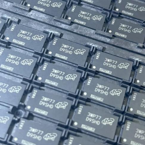





The MT41K256M16TW-107:P is a 4Gbit (256M x 16) DDR3L SDRAM manufactured by Micron Technology, operating at 1.35V with backward compatibility to 1.5V DDR3 platforms. It features an 8n-prefetch double data rate architecture supporting 1866 MT/s data rate (933 MHz clock) with CL=13 timing. The device incorporates 8 internal banks for concurrent operation, nominal and dynamic on-die termination (ODT), differential data strobe (DQS/DQS#), programmable CAS latency, burst length of 8 with burst chop 4 on-the-fly selection, self-refresh with temperature-compensated auto-refresh, write leveling, and ZQ calibration. Fabricated in 20nm process and packaged in a 96-ball FBGA (8mm x 14mm), it operates over the commercial temperature range of 0°C to 95°C, making it suitable for embedded computing, networking equipment, industrial automation, consumer electronics, and automotive infotainment systems.
Home » Dynamic Random Access Memory (DRAM), Integrated Circuits ICs » MT41K256M16TW-107:P
MT41K256M16TW-107:P
4Gbit DDR3L SDRAM, 1866 MT/s, 1.35V, 96-ball FBGA
Effective Inventory
Manufacturer Part:
MT41K256M16TW-107:P
Package:
96-ball FBGA (8mm x 14mm x 0.92mm)
Brand:
Product Categories:
Quality Commitment
Shipping & Payment
Service & Packaging
Product Manual
Other recommendations you may be interested in.
Description
Product Introduction: MT41K256M16TW-107:P Product Introduction
The MT41K256M16TW-107:P is a 4Gbit (512MB) DDR3L SDRAM device manufactured by Micron Technology, organized as 256 Meg x 16 bits. It belongs to the MT41K series of low-voltage DDR3 SDRAM devices, operating at VDD = VDDQ = 1.35V (range: 1.283V to 1.45V) while maintaining backward compatibility with 1.5V DDR3 applications. The device uses an 8n-prefetch architecture with a double data rate interface that transfers two data words per clock cycle at the I/O pins.
The -107 speed grade supports a maximum clock frequency of 933 MHz (1866 MT/s data rate) with CL = 13 timing (tRCD = 13.91ns, tRP = 13.91ns). The device incorporates 8 internal banks for concurrent operation, enabling high bandwidth by hiding row precharge and activation time. It features nominal and dynamic on-die termination (ODT) for data, strobe, and mask signals, differential bidirectional data strobe (DQS/DQS#), and differential clock inputs (CK/CK#).
Fabricated in 20nm process technology, the device is packaged in a 96-ball FBGA (8mm x 14mm, height 0.92mm) with commercial temperature range (0°C to 95°C). Key features include programmable CAS latency (CL), programmable posted CAS additive latency (AL), programmable CAS write latency (CWL), fixed burst length of 8 (BL8) and burst chop of 4 (BC4) with on-the-fly selection, self-refresh mode with temperature-compensated auto-refresh, write leveling, multipurpose register, and output driver calibration via ZQ pin. The device supports refresh intervals of 64ms at 0-85°C and 32ms at 85-95°C with 8192 refresh cycles.
Working Principle: MT41K256M16TW-107:P Working Principle
The MT41K256M16TW-107:P employs a double data rate (DDR) architecture based on an 8n-prefetch scheme. A single read or write operation consists of a single 8n-bit-wide, four-clock-cycle data transfer at the internal DRAM core, paired with eight corresponding n-bit-wide, one-half-clock-cycle data transfers at the I/O pins. This architecture enables high bandwidth while keeping the internal DRAM core frequency at one-eighth of the external data rate.
Clock and Command Subsystem: The device operates from differential clock inputs (CK and CK#). All control, command, and address signals are registered at the positive edge of CK. Commands are decoded from the CS#, RAS#, CAS#, WE#, and ACT# pins to initiate operations such as ACTIVATE, READ, WRITE, PRECHARGE, REFRESH, and mode register access.
Memory Array Subsystem: The 4Gbit density is organized as 256 Meg x 16 with 8 internal banks. Each bank contains 32K rows (A[14:0]), 1K columns (A[9:0]), and a 2KB page size. The 8-bank architecture allows concurrent bank operations, hiding row access latency through bank interleaving and improving overall throughput.
Data Path Subsystem: Data is transferred via the 16-bit DQ bus with differential data strobe signals (DQS/DQS#). During WRITE operations, DQS is center-aligned with data for reliable capture. During READ operations, the DRAM transmits data edge-aligned to DQS. The device supports BL8 (burst length 8) and BC4 (burst chop 4) with on-the-fly selection via the mode register.
On-Die Termination (ODT) Subsystem: The device supports both nominal and dynamic ODT for DQ, DQS, DQS#, and DM signals. ODT values are programmable through mode registers (RTT_NOM, RTT_WR), providing signal integrity optimization without external termination components. Dynamic ODT allows the termination value to change on-the-fly during write operations.
Refresh Subsystem: The device requires 8192 refresh commands every 64ms (0-85°C) or 32ms (85-95°C). Self-refresh mode with auto-refresh (SRT) enables autonomous refresh operation during low-power standby. The ZQ calibration subsystem performs periodic output driver impedance calibration against an external 240-ohm resistor to maintain signal integrity over temperature and voltage variations.
Pin Description: MT41K256M16TW-107:P Pin Definition and Functions
| Pin Group | Pin / Ball | Type | Default Function | Description |
|---|---|---|---|---|
| Clock | CK, CK# | I | Differential Clock Input | All commands are latched on the rising edge of CK |
| Chip Select | CS# | I | Chip Select (Active Low) | Enables or disables the command decoder |
| Command | RAS#, CAS#, WE# | I | Command Inputs | Define the command being entered along with CS# |
| Activate | ACT# | I | Activate Input | Activates the specified row in the selected bank |
| Address | A[14:0] | I | Address Inputs | Provide row and column address; also used for mode register set and burst chop |
| Bank Address | BA[2:0] | I | Bank Select | Select which bank is active for READ, WRITE, or ACTIVATE |
| Data | DQ[15:0] | I/O | Data Bus | Bi-directional data bus, 16-bit wide |
| Data Strobe | DQS, DQS# | I/O | Differential Data Strobe | Bi-directional differential strobe for data capture |
| Data Mask | DM | I | Data Mask Input | Masks write data; sampled during write operations |
| ODT | ODT | I | On-Die Termination Enable | Enables ODT for DQ/DQS/DM signals during reads |
| Clock Enable | CKE | I | Clock Enable (Active High) | Enables internal clock signals and device operation |
| Reset | RESET# | I | Active Low Reset | Asynchronous reset; clears all internal state |
| Calibration | ZQ | I | Impedance Calibration Reference | Connected to external 240-ohm resistor for ODT/driver calibration |
| Power | VDD | P | Core Power Supply | 1.35V nominal (1.283V – 1.45V) |
| Power | VDDQ | P | I/O Power Supply | 1.35V nominal (1.283V – 1.45V) |
| Power | VREFCA | P | Reference Voltage (CA) | Command/Address reference voltage = VDD/2 |
| Power | VREFDQ | P | Reference Voltage (DQ) | Data reference voltage = VDDQ/2 |
| Ground | VSS | G | Ground | Device ground connections |
Application Scenarios: In which products and applications is MT41K256M16TW-107:P used
| Application Scenario | Role of MT41K256M16TW-107:P | Key Features Utilized | Typical Pairing |
|---|---|---|---|
| Embedded Computing (ARM/FPGA Systems) | Main system memory providing 512MB capacity with high bandwidth for processor code execution and data buffering | 1866 MT/s data rate, 16-bit bus width, low 1.35V power, ODT for signal integrity | ARM Cortex-A series SoC (e.g., i.MX8, RK3399), FPGA (e.g., Xilinx Zynq UltraScale+) |
| Networking and Telecom Equipment | Packet buffering and lookup table storage in routers, switches, and baseband processors | 8-bank interleaving for concurrent access, BC4/BL8 on-the-fly, high MT/s throughput | Network SoC (e.g., NXP Layerscape), Ethernet switch ASIC |
| Industrial Automation and HMI | Operating system memory for industrial PCs, PLCs, and HMI panels requiring reliable DRAM in commercial temperature range | Self-refresh with auto-refresh (SRT), ZQ calibration, 0-95°C operation | Industrial MCU/MPU (e.g., TI Sitara, STM32MP1) |
| Consumer Electronics (Smart TV, STB) | Video frame buffer and application memory in smart TVs, set-top boxes, and streaming devices | 256Mx16 organization, low standby current, backward compatible with 1.5V DDR3 platforms | Media SoC (e.g., Realtek RTD1319, Amlogic S905X4) |
| Automotive Infotainment (Non-Safety) | System memory for in-vehicle infotainment (IVI) and navigation systems at commercial temperature grade | 1.35V low-power operation, write leveling, programmable ODT | Automotive SoC (e.g., Renesas R-Car, NXP i.MX8XL) |
Alternative Models: What chips are recommended as replacements for MT41K256M16TW-107:P
| Model | Compatibility Type | Compatibility Level | Key Differences | Manufacturer |
|---|---|---|---|---|
| AS4C256M16D3-12BCN | Functionally Similar | Partially Compatible | DDR3L 256Mx16, 1600 MT/s (slower), 96-ball FBGA, timing differences require firmware adjustment | Alliance Memory |
| IS46TR16256AL-15HBLA1-TR | Functionally Similar | Partially Compatible | DDR3L 256Mx16, 1333 MT/s, 96-ball FBGA, lower speed grade, requires timing reconfiguration | ISSI |
| MT41K256M16TW-107 IT:P | Series Variant | Fully Compatible | Industrial temp range (-40°C to 95°C), same speed grade and pinout, direct drop-in replacement for wider temp range | Micron |
| MT41K256M16TW-107 AIT:P | Series Variant | Fully Compatible | Automotive grade (AEC-Q100), -40°C to 95°C, higher unit price ($7.66+), same pinout and functionality | Micron |
| W632GU6MB-12 | Functionally Similar | Partially Compatible | DDR3L 256Mx16, 1600 MT/s, 96-ball FBGA, lower speed, different timing parameters | Winbond |
| EM6AB16CWKG-12H | Functionally Similar | Partially Compatible | DDR3L 256Mx16, 1600 MT/s, 96-ball FBGA, lower data rate, requires timing and mode register adjustments | Etron Technology |
Recommend Parts

ISL95855HRTZ-T
IMVP8 3+2+1 phase buck controller, R3 technology, 4.5-25V input, 48-TQFN
Brand: Renesas
Package: 48-TQFN (6×6 mm, exposed pad)
IN STOCK: 2156pcs
Cargo cycle: 3-7 Days
The minimum order is 1

IRFB4019PBF
150V N-Channel HEXFET Power MOSFET, 47A, 34 mΩ RDS(on), TO-220AB
Brand: infineon
Package: TO-220AB
IN STOCK: 2409pcs
Cargo cycle: 3-7 Days
The minimum order is 1

MSP430F247TPMR
TI MSP430 MCU, 16-bit RISC, 92KB Flash, 8KB RAM, 16MHz, LQFP-64
Brand: texas-instruments
Package: See datasheet
IN STOCK: 13371pcs
Cargo cycle: 3-7 Days
The minimum order is 1

UCC28740DR
CVCC Flyback Controller, 700V startup, opto feedback, <10mW no-load, SOIC-7
Brand: TI
Package: SOIC-7 (4.9 x 3.9 x 1.75 mm)
IN STOCK: 4840pcs
Cargo cycle: 3-7 Days
The minimum order is 1

MMUN2211LT1G
NPN digital transistor, R1=10kΩ R2=10kΩ, 50V, 100mA, SOT-23-3, pre-biased BRT switch
Brand: Onsemi
Package: SOT-23-3 (TO-236, SC-59)
IN STOCK: 8500pcs
Cargo cycle: 3-7 Days
The minimum order is 1

PIC32MX795F512L-80I/PF
32-bit PIC32MX MCU with Ethernet/CAN/USB, 80MHz, 512KB Flash, TQFP-100, industrial
Brand: MICROCHIP
Package: TQFP-100 (14 x 14 mm)
IN STOCK: 7912pcs
Cargo cycle: 3-7 Days
The minimum order is 1