
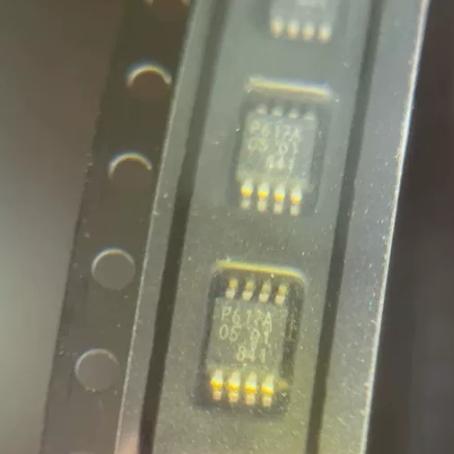





The PCA9617ADP from NXP Semiconductors is a level-translating Fast-mode Plus I2C-bus repeater in an 8-pin TSSOP package (3.0 x 4.4 mm). It provides bidirectional buffering and voltage level translation for I2C SDA and SCL lines between a low-voltage side (Port A: 0.8 V to 5.5 V, normal levels) and a higher-voltage side (Port B: 2.2 V to 5.5 V, static offset levels). The device supports clock frequencies from 0 Hz to 1000 kHz and enables two buses of 540 pF at 1 MHz or up to 4000 pF at lower speeds. Port B features a 0.55 V static offset for latch-free operation. Active-high enable input. 5 V tolerant I/O pins. ESD protection exceeds 5500 V HBM. -40°C to +85°C operating range.
Home » Integrated Circuits ICs, Interface ICs » PCA9617ADP
PCA9617ADP
Fm+ I2C repeater, 0.8-5.5V to 2.2-5.5V level shift, 1MHz, 540pF bus isolation, TSSOP-8, -40~85°C
4000
Effective Inventory
Manufacturer Part:
PCA9617ADP
Package:
TSSOP-8 (SOT505-1) (3.0 x 4.4 x 1.1 mm, 0.65mm pitch)
Brand:
Product Categories:
Quality Commitment
Shipping & Payment
Service & Packaging
Product Manual
Other recommendations you may be interested in.
Description
Product Introduction: PCA9617ADP Product Introduction
The PCA9617A is an I2C-bus repeater from NXP that provides both voltage level translation and bus capacitance isolation between two I2C bus segments. The PCA9617ADP is the TSSOP-8 packaged version, which is a footprint and functional replacement for the PCA9517A at Fast-mode speeds, with the added benefit of Fast-mode Plus (1 MHz) support.
The device has two ports with different voltage and signaling characteristics. Port A operates from 0.8 V to 5.5 V with normal CMOS logic levels — its output pulls down to near 0 V (hard low) and its input threshold is 0.35 × VCC(A). Port B operates from 2.2 V to 5.5 V with a static offset of approximately 0.55 V — its output pulls down to only 0.55 V, and its input threshold is about 0.45 V. The offset design prevents latch-up: when Port B internally drives low at 0.55 V, its own input (threshold 0.45 V) does not recognize this as a valid low, preventing the device from holding itself in a low state.
The key benefit of the PCA9617A is bus capacitance isolation. Each port of the repeater presents only about 7 pF of capacitance to its respective bus, regardless of the capacitance on the other side. This allows system designers to create large I2C networks well beyond the 400-pF specification limit. At 1 MHz (Fm+), each side can support up to 540 pF; at lower speeds, each side can support up to 4000 pF.
The level translation works in both directions without direction pins — the open-drain I2C bus architecture inherently supports this. A low on Port A (below 0.3 × VCC(A)) turns on the Port B pull-down. A low on Port B (below 0.4 V) turns on the Port A pull-down. This bidirectional operation is transparent to the I2C protocol, including arbitration, clock stretching, and multi-master scenarios.
The EN (enable) pin is active-high, referenced to VCC(B). When EN is low, both port drivers are disabled and all I/O pins are high-impedance. The device is enabled only when VCC(A) > 0.8 V and VCC(B) > 2.2 V, with a ~400 µs power-up delay for internal reference settling.
The PCA9617A is included in NXP’s 15-year product longevity program, making it suitable for long-lifecycle industrial and automotive applications.
Working Principle: PCA9617ADP Working Principle
**Bidirectional Open-Drain Buffering:** The PCA9617A implements two identical channels (SDA and SCL), each consisting of a pair of open-drain buffers connected back-to-back between Port A and Port B. Because I2C is an open-drain bus, there is no need for direction control signals — the bus itself determines the direction of data flow.
**Port A to Port B Translation:** When a device on Port A pulls SDA_A below 0.3 × VCC(A), the Port B driver activates and pulls SDA_B down to approximately 0.55 V (not to 0 V, due to the static offset). When SDA_A rises above the threshold, the Port B driver releases and the external pull-up resistor on SDA_B pulls it high.
**Port B to Port A Translation:** When a device on Port B pulls SDA_B below 0.4 V, the Port A driver activates and pulls SDA_A down to near 0 V (hard low). When SDA_B rises above 0.4 V, the Port A driver releases. The hard low on Port A is critical for low-voltage operation, as it maximizes the noise margin at 0.8 V.
**Static Offset and Latch Prevention:** The 0.55-V offset on Port B means that when the PCA9617A internally drives Port B low, the resulting 0.55-V level is above the Port B input threshold (0.45 V? — no, the internal buffer input is 90 mV below the output, at ~0.45 V). Actually, the input threshold is set 90 mV below the output pull-down level: output drives to 0.55 V, input threshold is 0.45 V. So the internally generated 0.55 V is NOT recognized as a low by the input (since it’s above 0.45 V). This prevents the latch condition where the device would hold itself low indefinitely.
**Capacitance Isolation:** Each port presents only ~7 pF loading to its bus. The buffering action means that the capacitance on one bus does not add to the other. Rise times on each bus are determined only by the pull-up resistor and capacitance on that side, not by the total system capacitance.
Pin Description: PCA9617ADP Pin Definition and Functions
| Pin | Name | Type | Description |
|---|---|---|---|
| 1 | SCL_A | I/O | Port A I2C clock; open-drain I/O; 0.8-5.5V; 5V tolerant; 7pF typical capacitance; hard low output (~0V) |
| 2 | SDA_A | I/O | Port A I2C data; open-drain I/O; same characteristics as SCL_A |
| 3 | VCC(A) | P | Port A supply; 0.8V to 5.5V; bypass with 0.1µF; must be >0.8V for enable |
| 4 | GND | G | Ground; connect to PCB ground plane |
| 5 | EN | I | Enable input; active-high; referenced to VCC(B); drive high to enable repeater; low disables both drivers; only change when bus idle |
| 6 | SCL_B | I/O | Port B I2C clock; open-drain I/O; 2.2-5.5V; 5V tolerant; static offset output (~0.55V) |
| 7 | SDA_B | I/O | Port B I2C data; open-drain I/O; same characteristics as SCL_B |
| 8 | VCC(B) | P | Port B supply; 2.2V to 5.5V; bypass with 0.1µF; must be >2.2V for enable; EN pin referenced to this supply |
Application Scenarios: In which products and applications is PCA9617ADP used
| Application | Description |
|---|---|
| Multi-Voltage I2C Sensor Network | Connect 1.8V MCU I2C bus (Port A) to 5V sensor bus (Port B); bidirectional level translation without direction pins; 540pF isolation allows many sensors on 5V side; EN pin for bus isolation during MCU sleep |
| Long-Distance I2C Extension | Extend I2C bus beyond 400pF limit by splitting into two segments; local bus (low capacitance, Port A) and remote bus (high capacitance cable, Port B); 4000pF support at 100kHz allows cable lengths of 10+ meters; pair with P82B96 for even longer runs |
| Hot-Swap I2C Card Isolation | Isolate backplane I2C bus (Port B) from plug-in card I2C (Port A); capacitance isolation protects backplane from card insertion transients; powered-off high-impedance prevents card from loading bus when unpowered; EN pin controlled by card-detect signal |
Alternative Models: What chips are recommended as replacements for PCA9617ADP
| Model | Manufacturer | Compatibility | Key Difference |
|---|---|---|---|
| PCA9517ADP | NXP | Footprint-Compatible Predecessor | Same TSSOP-8 pinout; Fm (400kHz) only vs Fm+ (1MHz); lower max frequency; use for legacy designs that don’t need Fm+ speed |
| PCA9617ATP | NXP | Series Variant (HWSON8) | Same function in HWSON8 (2x3mm) package; smaller footprint; no leads; use for space-constrained designs |
| TCA9406DCUR | TI | Functional Equivalent | 2-channel I2C level translator; 1.65-3.6V to 2.7-5.5V; 1MHz Fm+; VSSOP-8; different offset architecture; verify compatibility for multi-repeater designs |
| LTC4311IDDB#TRMPBF | ADI | Competitive Alternative | I2C bus accelerator (rise-time accelerator); not a level translator; DFN-8; use when only rise-time improvement needed without voltage translation |
Recommend Parts

ISL95855HRTZ-T
IMVP8 3+2+1 phase buck controller, R3 technology, 4.5-25V input, 48-TQFN
Brand: Renesas
Package: 48-TQFN (6×6 mm, exposed pad)
IN STOCK: 2156pcs
Cargo cycle: 3-7 Days
The minimum order is 1

IRFB4019PBF
150V N-Channel HEXFET Power MOSFET, 47A, 34 mΩ RDS(on), TO-220AB
Brand: infineon
Package: TO-220AB
IN STOCK: 2409pcs
Cargo cycle: 3-7 Days
The minimum order is 1

MSP430F247TPMR
TI MSP430 MCU, 16-bit RISC, 92KB Flash, 8KB RAM, 16MHz, LQFP-64
Brand: texas-instruments
Package: See datasheet
IN STOCK: 13371pcs
Cargo cycle: 3-7 Days
The minimum order is 1

UCC28740DR
CVCC Flyback Controller, 700V startup, opto feedback, <10mW no-load, SOIC-7
Brand: TI
Package: SOIC-7 (4.9 x 3.9 x 1.75 mm)
IN STOCK: 4840pcs
Cargo cycle: 3-7 Days
The minimum order is 1

MMUN2211LT1G
NPN digital transistor, R1=10kΩ R2=10kΩ, 50V, 100mA, SOT-23-3, pre-biased BRT switch
Brand: Onsemi
Package: SOT-23-3 (TO-236, SC-59)
IN STOCK: 8500pcs
Cargo cycle: 3-7 Days
The minimum order is 1

PIC32MX795F512L-80I/PF
32-bit PIC32MX MCU with Ethernet/CAN/USB, 80MHz, 512KB Flash, TQFP-100, industrial
Brand: MICROCHIP
Package: TQFP-100 (14 x 14 mm)
IN STOCK: 7912pcs
Cargo cycle: 3-7 Days
The minimum order is 1