



Opens in a new tab

Home » Connectors & Interconnect Devices » 8A34001E-000AJG8

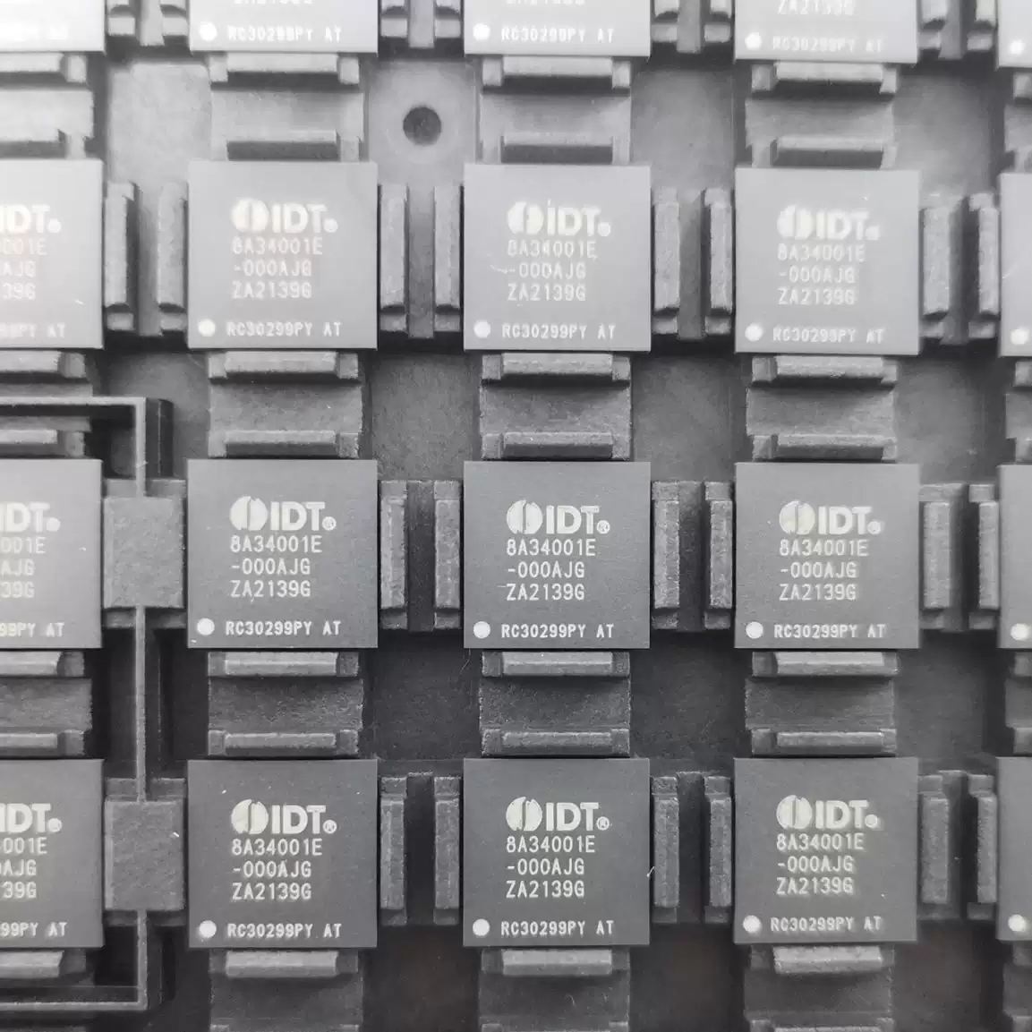
8A34001E-000AJG8

ClockMatrix 8-channel system synchronizer, IEEE 1588 PTP + SyncE, 8 DPLL/DCO, 150fs jitter, 144-CABGA 10x10mm, Renesas/IDT, G.8273.2 Class D

2598

Effective Inventory

Image for reference only

Manufacturer Part:

8A34001E-000AJG8

Package:

144-CABGA (chip array ball grid array, 10x10mm body, 0.8mm ball pitch, 12×12 ball array, 4-sided perimeter + inner row)

Brand:

Quality Commitment

Shipping & Payment

Service & Packaging

Product Manual

Description

Product Overview

The 8A34001E-000AJG8 is a high-performance Synchronization Management Unit (SMU) from Renesas Electronics, part of the ClockMatrix family. This 8-channel system synchronizer generates ultra-low jitter precision timing signals based on the IEEE 1588 Precision Time Protocol (PTP) and Synchronous Ethernet (SyncE), enabling sub-microsecond time synchronization in packet-based and physical layer equipment.

The device provides eight independent timing channels, each configurable as a frequency synthesizer, jitter attenuator, Digitally Controlled Oscillator (DCO), or Digital Phase Lock Loop (DPLL). DPLLs comply with ITU-T G.8262 for Synchronous Ethernet and support legacy SONET/SDH and PDH requirements. DCOs can synthesize PTP/IEEE 1588 clocks with frequency resolution better than 1.11 x 10⁻¹⁶, making them ideal for Telecom Boundary Clock (T-BC) and Telecom Time Slave Clock (T-TSC) applications per ITU-T G.8273.2.

Housed in a 144-ball chip array BGA (CABGA) package measuring just 10 x 10 mm with 0.8 mm pitch, the 8A34001 delivers up to 12 differential or 24 LVCMOS outputs at frequencies from 0.5 Hz to 1 GHz. RMS jitter is below 150 fs typical (10 kHz to 20 MHz), supporting 100GBASE-R, 40GBASE-R, and lower-rate Ethernet interfaces as well as SONET/SDH, PDH, CPRI/OBSAI, and IEEE 1588 Time Stamp Units (TSUs). The device operates from 1.71 V to 3.465 V supply over the -40 degC to +85 degC industrial temperature range.

Key Specifications

Parameter Value
Device Type Clock Synchronizer / SMU (Synchronization Management Unit)
Timing Channels 8 independent (DPLL / DCO / Synthesizer / Jitter Attenuator)
Clock Inputs 8 differential / 16 single-ended (0.5 Hz to 1 GHz)
Clock Outputs 12 differential / 24 LVCMOS (0.5 Hz to 1 GHz, 250 MHz LVCMOS max)
Output Jitter < 150 fs RMS typical (10 kHz to 20 MHz)
DPLL Loop Bandwidth 12 microHz to 22 kHz (programmable)
DCO Frequency Resolution < 1.11 x 10^-16 (sub-ppt)
Phase Tuning Resolution 1 ps (per FOD output)
TDC Resolution < 1 ps (DPLL phase detectors)
Input-to-Output Phase Offset Up to +-1.638 micro-s per input, 1 ps steps
Output Standards LVCMOS, LVDS, LVPECL, HCSL, CML, SSTL, HSTL
Differential Output Swing 400 / 650 / 800 / 910 mV (selectable)
Output Voltage Options 3.3 V, 2.5 V, 1.8 V (LVCMOS: +1.5 V, 1.2 V)
System APLL Reference 25 MHz to 54 MHz crystal / XO
System DPLL XO Input 1 MHz to 150 MHz (XO/TCXO/OCXO)
Supply Voltage 1.71 V to 3.465 V
Standards Compliance ITU-T G.8262 (SyncE), G.8273.2 (T-BC/T-TSC), G.8263, G.8264
Serial Interface I2C (1 MHz) / SPI (50 MHz)
Configuration OTP (16 configs) / External I2C EEPROM / JTAG
Operating Temperature -40 degC to +85 degC
Package 144-CABGA (10 x 10 mm, 0.8 mm pitch)

Features

  • 8 independent timing channels: DPLL, DCO, frequency synthesizer, or jitter attenuator
  • IEEE 1588 PTP support via DCO mode with sub-ppt frequency resolution
  • ITU-T G.8262 compliant SyncE EEC options 1 and 2
  • ITU-T G.8273.2 T-BC / T-TSC Class C/D compliant
  • Combo Bus for DPLL/DCO frequency sharing (G.8273.2 support)
  • Hitless, dynamic switching between DPLL and DCO modes
  • Ultra-low jitter: <150 fs RMS typical (10 kHz – 20 MHz)
  • 12 differential outputs / 24 LVCMOS outputs, 0.5 Hz to 1 GHz
  • 8 differential / 16 single-ended inputs, 0.5 Hz to 1 GHz
  • Any input mappable to any or all timing channels
  • Fractional Output Dividers (FODs) with 1 ps phase tuning
  • Per-input programmable phase offset: +-1.638 micro-s in 1 ps steps
  • Reference monitors: LOS, activity, frequency monitoring
  • Automatic reference selection with priority tables
  • Revertive / non-revertive reference switching
  • Supports sync pulses: 1PPS, 5PPS, 10PPS, EPPS, 50Hz-8kHz
  • System APLL: 25-54 MHz crystal or XO
  • System DPLL: 1 MHz-150 MHz XO/TCXO/OCXO input
  • I2C (1 MHz) and SPI (50 MHz) serial processor ports
  • Internal OTP memory: up to 16 customer configurations
  • External I2C EEPROM auto-configuration support
  • JTAG boundary scan (1149.1)
  • 144-CABGA 10 x 10 mm package, 0.8 mm pitch
  • RoHS compliant, MSL 3, industrial temperature range

Applications

  • 5G NR O-RAN radio units and base stations
  • Core and access IP switches and routers
  • Synchronous Ethernet (SyncE) equipment
  • Telecom Boundary Clocks (T-BC) and T-TSCs
  • 10G / 40G / 100G Ethernet interface synchronization
  • Central office timing source and distribution
  • Wireless infrastructure (4.5G and 5G)
  • IEEE 1588 PTP grandmaster and slave clocks
  • SONET / SDH / PDH network equipment
  • CPRI / OBSAI wireless base station interfaces
  • PTP time cards for data centers
  • High-speed SERDES reference clocks (up to 28 Gbps)

Product Introduction: 8A34001E-000AJG8 Product Introduction

The 8A34001E-000AJG8 is an 8-channel System Synchronizer for IEEE 1588 from Renesas Electronics’ ClockMatrix family. Formerly developed by Integrated Device Technology (IDT, acquired by Renesas in 2019), this device is a highly integrated Synchronization Management Unit (SMU) designed for packet-based and physical-layer based equipment synchronization.

At its core, the 8A34001 provides eight independent timing channels that can each be configured as a Digital Phase Lock Loop (DPLL), Digitally Controlled Oscillator (DCO), frequency synthesizer, or jitter attenuator. This multi-channel architecture enables simultaneous support for IEEE 1588 PTP clock synthesis, Synchronous Ethernet (SyncE) clock generation, jitter attenuation, and universal frequency translation – all in a single 10 x 10 mm CABGA package.

The DPLLs comply with ITU-T G.8262 for Synchronous Ethernet Equipment Clock (EEC) options 1 and 2, and also support legacy SONET/SDH and PDH requirements. The DPLL Digital Loop Filters are programmable with cutoff frequencies from 12 microHz to 22 kHz, supporting applications from 1PPS synchronization to high-frequency jitter attenuation.

For IEEE 1588 PTP applications, the DCO mode offers frequency resolution better than 1.11 x 10^-16 (sub-ppt), enabling highly precise clock steering by external PTP servo software. The Combo Bus feature allows DPLL/DCO channels to share frequency information, simplifying compliance with ITU-T G.8273.2 for Telecom Boundary Clocks (T-BC) and Telecom Time Slave Clocks (T-TSC). Switching between DPLL and DCO modes is hitless and dynamic.

The device delivers ultra-low jitter outputs below 150 fs RMS (typical), making them suitable for synchronizing high-speed SERDES interfaces up to 28 Gbps including 100GBASE-R, 40GBASE-R, 10GBASE-R, and 10GBASE-W, as well as SONET/SDH, PDH, CPRI/OBSAI, and IEEE 1588 Time Stamp Units.

Input flexibility is exceptional: 8 differential/16 single-ended clock inputs accepting frequencies from 0.5 Hz to 1 GHz, with any input mappable to any or all timing channels. Output versatility matches: 12 differential/24 LVCMOS outputs from 0.5 Hz to 1 GHz, supporting LVCMOS, LVDS, LVPECL, HCSL, CML, SSTL, and HSTL standards with selectable output swing and independent supply voltages.

The 8A34001E variant (suffix -000AJG8) offers Class D performance for G.8273.2, the highest class available. The device is used in the AMD Zynq UltraScale+ RFSoC DFE ZCU670 evaluation kit as the timing platform for 5G NR O-RAN reference designs.

Working Principle: 8A34001E-000AJG8 Working Principle

The 8A34001 is a digital-intensive Synchronization Management Unit that combines analog PLL technology with digital signal processing to achieve precise clock synchronization. Here is how the key architectural blocks work together:

1. System APLL and Reference Clock: The System Analog PLL generates a high-frequency internal clock from an external 25-54 MHz crystal or oscillator. This APLL output feeds the Fractional Output Dividers (FODs) that synthesize all output frequencies. The high-frequency reference ensures that even fractional-N division produces low-jitter outputs across the entire 0.5 Hz to 1 GHz output range.

2. System DPLL: The System DPLL generates a stable internal system clock used by reference monitors and digital circuitry. It can free-run on the system APLL reference or lock to an external XO/TCXO/OCXO (1 MHz to 150 MHz) for higher stability. The system clock stability directly determines DPLL performance in Free-Run and Holdover modes.

3. Eight DPLL/DCO Channels: Each of the eight timing channels contains a Digital PLL that can operate in four modes:
– Free-Run: Output frequency based solely on the system clock
– Locked: DPLL filters reference jitter at the selected bandwidth
– Holdover: Maintains output frequency using historical data from Locked mode when references fail
– DCO: Opens the loop, allowing external PTP servo software to steer the output frequency

DPLL loop filter bandwidth is programmable from 12 microHz to 22 kHz. Very low bandwidths (below 20 mHz) enable direct locking to 1PPS references. Mid-bandwidths (0.05-0.1 Hz) serve G.8273.2 PTP applications. Higher bandwidths (0.1-10 Hz) handle G.8262 SyncE and SONET/SDH. Bandwidths above 10 Hz are used for jitter attenuation.

4. Reference Inputs and Monitoring: Up to 8 differential (16 single-ended) input clocks are continuously monitored for loss-of-signal, activity, and frequency offset against programmable thresholds. Automatic reference selection state machines switch the active reference based on priority tables, revertive/non-revertive settings, and monitor status. Any input can be designated as a sync/frame pulse (1PPS, EPPS, 5PPS, 10PPS, 50Hz-8kHz) associated with a selectable clock reference.

5. Fractional Output Dividers (FODs): Each output channel uses a fractional divider to generate any output frequency independent of the input frequency. FODs also support output phase tuning with 1 ps resolution, enabling precise phase alignment across multiple outputs and precise skew adjustment. Output phase can be adjusted over a full +-180 degree range.

6. Combo Bus for T-BC Operation: In Telecom Boundary Clock applications per ITU-T G.8273.2, one DPLL operates as a SyncE EEC (physical layer frequency reference) while another operates as a PTP DCO. The Combo Bus allows the DCO to use the EEC’s frequency as a stable reference, improving PTP clock stability and simplifying G.8273.2 compliance. Switching between DPLL and DCO modes is hitless.

7. Configuration and Interfaces: The device is configured through I2C (up to 1 MHz) or SPI (up to 50 MHz) slave interfaces. At power-up, configuration can be automatically loaded from internal One-Time Programmable (OTP) memory (up to 16 configurations) or from an external I2C EEPROM via a dedicated I2C master port. JTAG boundary scan is also supported.

Pin Description: 8A34001E-000AJG8 Pin Definition and Functions
Pin Group Pin Name(s) Type Description
Power VDDD (Core) Power Digital core supply voltage: 1.8 V typical (1.71 V to 1.89 V). Multiple VDDD balls – all must be connected with proper decoupling.
Power VDDA (Analog) Power Analog supply for APLL and sensitive circuits: 2.5 V or 3.3 V. Requires careful filtering for low jitter performance.
Power VDDO_Q0-Q11 Power Output bank supply voltages. Each group of outputs has its own VDDO. Supports 3.3 V, 2.5 V, or 1.8 V. LVCMOS outputs also support 1.5 V and 1.2 V.
Power VCC_GPIO_DC Power GPIO and digital I/O supply: 2.5 V or 3.3 V. Determines I/O voltage levels for control pins.
Ground GND / VSS Ground Ground reference. Multiple ground balls distributed throughout the package for signal integrity and thermal dissipation.
Clock Inputs CLK[0:7] / nCLK[0:7] Input 8 differential clock input pairs. Each pair can be used as one differential clock or two single-ended clocks. Frequency range: 0.5 Hz to 1 GHz (diff) / 250 MHz (single-ended).
Clock Outputs Q[0:11] / nQ[0:11] Output 12 differential clock output pairs. Each pair can be one differential or two LVCMOS outputs. Output frequency: 0.5 Hz to 1 GHz (diff) / 250 MHz (LVCMOS). Configurable standards: LVDS, LVPECL, HCSL, CML, SSTL, HSTL, LVCMOS.
Crystal / XO OSCI, OSCO I/O Crystal oscillator interface. Connect 25-54 MHz fundamental mode crystal between OSCI and OSCO, or drive OSCI with external XO reference.
XO DPLL Ref XODPLL / nXODPLL Input Differential input for System DPLL reference (XO/TCXO/OCXO). Supports 1 MHz to 150 MHz. Optional, for applications requiring high-stability local oscillator.
GPIO GPIO[0:15] I/O General-purpose I/O pins. Many have alternate functions including additional clock inputs, status outputs, LOS indicators, interrupts, and control signals. Some GPIO pins can serve as alternate clock inputs (CLK8-CLK15).
I2C Interface SDA, SCL I/O I2C serial interface data and clock. Up to 1 MHz operation. Used for device configuration and status monitoring. I2C Master port also available for EEPROM boot.
SPI Interface SCLK, SDIO, SDO, CS I/O SPI serial interface. Up to 50 MHz clock. Alternative to I2C for device configuration and register access.
JTAG TCK, TMS, TDI, TDO I/O JTAG boundary scan interface (IEEE 1149.1). For production test and boundary scan testing.
Reset RST_N Input Active-low hardware reset input. Assert low to reset all registers and state machines to default values.
Control I2C_SPI_SEL Input Interface select pin. Selects between I2C and SPI serial processor interface operation.
Status INT_N Output Interrupt output (active low). Asserts when status events occur (reference fail, lock change, etc.). Open drain, requires pull-up.

Package: 144-CABGA (Chip Array Ball Grid Array). Body dimensions: 10.0mm x 10.0mm x 1.2mm. Ball pitch: 0.8mm. Ball array: approximately 12 x 12 grid (perimeter + some inner rows). 4-side perimeter I/O arrangement. RoHS compliant, lead-free solder balls. MSL Level 3. Operating temperature: -40 degC to +85 degC.

Application Scenarios: In which products and applications is 8A34001E-000AJG8 used
  • 5G NR O-RAN Radio Units and Base Stations: Precision timing for 5G new radio access networks, including O-RAN radio units (O-RUs) and distributed units (O-DUs). The 8A34001 provides T-BC functionality per ITU-T G.8273.2 Class C/D, combining SyncE physical layer frequency with IEEE 1588 PTP packet timing. Verified in AMD Zynq UltraScale+ RFSoC DFE ZCU670 reference designs for O-RAN S-plane requirements.
  • Telecom Boundary Clocks (T-BC) and Time Slave Clocks (T-TSC): Core component of telecom-grade PTP clocks complying with ITU-T G.8273.2. The dual DPLL/DCO architecture with Combo Bus enables physical layer frequency assist from SyncE to improve PTP clock stability, meeting stringent time and phase error requirements for Class C and Class D performance levels.
  • Synchronous Ethernet (SyncE) Equipment: Synchronous Ethernet Equipment Clock (EEC) generation compliant with ITU-T G.8262 options 1 and 2. Used in carrier-grade switches and routers to distribute physical layer frequency synchronization across network elements, supporting wander generation, noise tolerance, and transient response requirements.
  • Core and Access IP Switches/Routers: High-speed network switching equipment requiring multiple synchronized clock domains. The 8 independent channels can simultaneously generate clocks for 10G/40G/100G Ethernet interfaces, SONET/SDH framers, and system logic, all phase-aligned and synchronized to network references.
  • Central Office Timing Source and Distribution: Building integrated timing supply (BITS) and central office clock distribution systems. The device serves as a Synchronous Equipment Timing Source (SETS) per ITU-T G.8264, generating T0 and T4 reference clocks for transmission equipment, with full redundancy and hitless reference switching.
  • IEEE 1588 PTP Grandmaster and Slave Clocks: Precision Time Protocol grandmaster clocks and slave clocks for industrial automation, power utility, and financial trading networks. DCO mode with sub-ppt frequency resolution allows precise clock steering by PTP servo algorithms, while ultra-low jitter outputs feed high-speed time stamp units (TSUs) for nanosecond-level time stamping.
  • CPRI/OBSAI Wireless Base Station Interfaces: Clock generation for Common Public Radio Interface (CPRI) and Open Base Station Architecture Initiative (OBSAI) links between baseband units and remote radio heads. The low jitter performance ensures error-free transmission at high line rates across optical and electrical interfaces.
  • PTP Time Cards for Data Centers: Precision timing cards for data center and financial trading applications requiring sub-microsecond time synchronization across distributed compute nodes. The device generates low-jitter clocks for network PHYs and MACs while the DCO steers time alignment based on PTP grandmaster feedback.
Alternative Models: What chips are recommended as replacements for 8A34001E-000AJG8
Manufacturer Part Number Channels Max Freq Jitter DPLL/DCO Package Notes
Renesas 8A34001E-000AJG 8 1 GHz 150 fs RMS 8 DPLL/DCO 144-CABGA Tray version (not reel)
Renesas 8A34001C-000AJG8 8 1 GHz 200 fs RMS 8 DPLL/DCO 144-CABGA Standard grade, lower cost
Renesas 8A34001B-000AJG8 8 1 GHz 200 fs RMS 8 DPLL/DCO 144-CABGA Base variant
Renesas 8A34002-000NJGI8 4 1 GHz 150 fs RMS 4 DPLL/DCO 48-QFN 4-channel, smaller package
Renesas RC31008A 8 1 GHz 120 fs RMS FemtoClock 72-QFN FemtoClock 2, newer gen
Texas Instruments LMK5C33414 3 1.25 GHz 40 fs BAW 3 DPLL+APLL 64-VQFN BAW VCO, lower jitter
Texas Instruments LMK05318B 1 1.25 GHz 50 fs BAW 1 DPLL+2 APLL 48-VQFN Single DPLL, BAW based
Microchip ZL30723 3 1 GHz 250 fs RMS 3 DPLL 64-VFQFN 3 DPLL, SyncE/PTP

Recommend Parts

ISL95855HRTZ-T

IMVP8 3+2+1 phase buck controller, R3 technology, 4.5-25V input, 48-TQFN

Brand: Renesas

Package: 48-TQFN (6×6 mm, exposed pad)

IN STOCK: 2156pcs

Cargo cycle: 3-7 Days

The minimum order is 1

IRFB4019PBF

150V N-Channel HEXFET Power MOSFET, 47A, 34 mΩ RDS(on), TO-220AB

Brand: infineon

Package: TO-220AB

IN STOCK: 2409pcs

Cargo cycle: 3-7 Days

The minimum order is 1

MSP430F247TPMR

TI MSP430 MCU, 16-bit RISC, 92KB Flash, 8KB RAM, 16MHz, LQFP-64

Package: See datasheet

IN STOCK: 13371pcs

Cargo cycle: 3-7 Days

The minimum order is 1

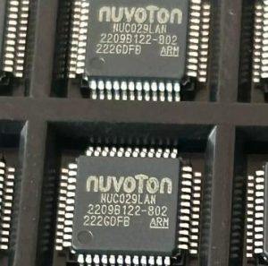
NUC029LAN

ARM Cortex-M0 MCU, 50MHz, 64KB Flash, 4KB SRAM, dual UART/SPI/I2C, LQFP-48

Brand: Nuvoton

Package: LQFP-48 (7.0 x 7.0 x 1.45 mm)

IN STOCK: 12385pcs

Cargo cycle: 3-7 Days

The minimum order is 1

AT45DB081E-SHN-T

8Mbit DataFlash, dual-SPI 85MHz, 2x264B SRAM buffers, USON-8 (4x3mm), page-based ECC

Brand: Renesas

Package: USON-8 (4 x 3 x 0.6mm, 0.8mm pitch)

IN STOCK: 4500pcs

Cargo cycle: 3-7 Days

The minimum order is 1

PIC32MX795F512L-80I/PF

32-bit PIC32MX MCU with Ethernet/CAN/USB, 80MHz, 512KB Flash, TQFP-100, industrial

Brand: MICROCHIP

Package: TQFP-100 (14 x 14 mm)

IN STOCK: 7912pcs

Cargo cycle: 3-7 Days

The minimum order is 1