
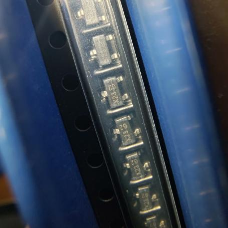


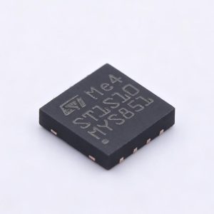


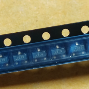
The BSS123-7-F is an N-channel enhancement mode trench MOSFET from Diodes Incorporated featuring 100 V drain-source voltage, 170 mA continuous drain current, 6 Ω RDS(on) at VGS = 10 V, and VGS(th) of 2.0 V max. With 60 pF input capacitance, 300 mW power dissipation, and AEC-Q101 qualification, it is ideal for low-side load switching, logic level shifting, and general-purpose digital control. Packaged in SOT-23-3 (2.9 x 1.3 mm) with MSL-1 rating and Pb-free compliance, it operates over -55°C to +150°C junction temperature. Supplied in tape and reel (3000 units/reel).
Home » Integrated Circuits ICs, MOSFETs » BSS123-7-F
BSS123-7-F
N-channel enhancement MOSFET, 100V, 170 mA, 6 Ω RDS(on), SOT-23-3, AEC-Q101
207116
Effective Inventory
Manufacturer Part:
BSS123-7-F
Package:
SOT-23-3 (2.9 x 1.3 mm)
Brand:
Product Categories:
Quality Commitment
Shipping & Payment
Service & Packaging
Product Manual
Other recommendations you may be interested in.
Description
Product Introduction: BSS123-7-F Product Introduction
The BSS123-7-F is an N-channel enhancement mode MOSFET manufactured by Diodes Incorporated, utilizing proprietary high-density trench technology. It features a drain-source breakdown voltage (VDSS) of 100 V, continuous drain current (ID) of 170 mA at 25°C ambient, and on-resistance (RDS(on)) of 6 Ω maximum at VGS = 10 V and ID = 170 mA. The gate-source threshold voltage (VGS(th)) is 2.0 V maximum at ID = 1 mA.
Key electrical characteristics include a maximum gate-source voltage of ±20 V, input capacitance (Ciss) of 60 pF maximum at VDS = 25 V, and power dissipation of 300 mW at 25°C ambient. The device operates over a junction temperature range of -55°C to +150°C.
The BSS123-7-F is packaged in the industry-standard SOT-23-3 (TO-236-3, SC-59) package with dimensions of 2.9 x 1.3 x 1.0 mm. It features a matte tin finish annealed over alloy 42 lead frame, UL94V-0 flame-rated molded plastic case, and is MSL-1 rated (unlimited floor life). The -7 suffix denotes tape and reel packaging (3000 units per reel), and the -F suffix indicates green (Pb-free) compliance. The device is also AEC-Q101 qualified for automotive applications.
The low gate threshold voltage, low input capacitance, and fast switching speed make this MOSFET ideal for low-voltage and low-current switching applications such as level shifting, load switching, and general-purpose digital control.
Working Principle: BSS123-7-F Working Principle
The BSS123-7-F is an N-channel enhancement mode MOSFET that operates by modulating the conductivity of a channel between source and drain using an electric field applied to the gate terminal.
Enhancement Mode Operation: With no gate-source voltage applied (VGS = 0 V), the MOSFET is in the off state. There is no conductive channel between drain and source, and only a tiny leakage current (IDSS) flows. This is the normally-off characteristic of enhancement mode devices.
Channel Formation: When a positive gate-source voltage exceeding the threshold voltage (VGS(th)) is applied, the electric field attracts electrons to the semiconductor surface beneath the gate oxide, forming an inversion layer (conducting channel) between source and drain. For the BSS123-7-F, VGS(th) is typically around 1.0-1.4 V, with a maximum of 2.0 V at ID = 1 mA.
Ohmic (Linear) Region: At low VDS, the drain current is approximately proportional to VDS, and the channel behaves like a resistor with value RDS(on). The RDS(on) is 6 Ω maximum at VGS = 10 V. Higher VGS increases the channel charge density, reducing RDS(on) and increasing drain current capability.
Saturation Region: At higher VDS, the channel pinches off near the drain end, and the drain current becomes relatively independent of VDS, limited by the gate voltage. The device acts as a current source in this region.
Switching Behavior: The MOSFET is voltage-driven and requires virtually no steady-state gate current (only the gate leakage current, typically less than 100 nA). The switching speed is determined by the time required to charge and discharge the input capacitance (Ciss = 60 pF max) through the gate driver impedance. The low Ciss enables fast turn-on and turn-off transitions, making the device suitable for high-frequency switching applications.
Trench Technology: The BSS123-7-F uses trench MOSFET technology, where the gate structure is formed vertically in a trench etched into the silicon. This approach reduces cell size and increases channel density per unit area, achieving lower RDS(on) for a given die size compared to planar MOSFET construction.
Pin Description: BSS123-7-F Pin Definition and Functions
| Pin | Name | Type | Default Function | Description |
|---|---|---|---|---|
| 1 | Gate | I | Gate Control Input | Voltage-controlled input; drives channel formation between drain and source; high impedance DC input |
| 2 | Source | G | Source Terminal | Current source terminal; typically connected to ground in low-side switch configuration |
| 3 | Drain | O | Drain Terminal | Current drain terminal; connects to load in switching applications |
Application Scenarios: In which products and applications is BSS123-7-F used
| Application | Description |
|---|---|
| Low-Side Load Switch | Switching resistive or inductive loads such as LEDs, relays, and small motors with gate drive from 3.3V or 5V logic |
| Logic Level Shifting | Bi-directional or unidirectional voltage level translation between 3.3V and 5V logic domains in mixed-voltage systems |
| Battery-Powered Device Control | Power gating and sleep-mode control in portable devices; low gate threshold enables operation from single-cell lithium supplies |
| Automotive Body Electronics | AEC-Q101 qualified switching for interior lighting, door lock actuators, and sensor signal conditioning in automotive body control modules |
| General-Purpose Digital Control | Microcontroller GPIO expansion for driving loads beyond direct GPIO current capability; 100V rating provides margin for inductive kickback |
Alternative Models: What chips are recommended as replacements for BSS123-7-F
| Model | Manufacturer | Compatibility | Key Difference |
|---|---|---|---|
| BSS123 | NXP / Various | Pin-Compatible | Industry-standard equivalent; same pinout and similar specs; verify RDS(on) and VGS(th) matching for specific manufacturer |
| 2N7002 | Various | Pin-Compatible | 60V, 115 mA, 1.2-2.8 Ω RDS(on); lower voltage, lower RDS(on), different VGS(th) range; most common small-signal MOSFET alternative |
| MMBF170 | onsemi | Pin-Compatible | 60V, 500 mA; higher current rating, lower RDS(on); different threshold voltage characteristics |
| BSS138 | Diodes Incorporated / Various | Pin-Compatible | 50V, 220 mA, 3.5 Ω RDS(on); lower voltage, lower RDS(on), popular for level shifting |
| DMN2075U | Diodes Incorporated | Functionally Similar | 20V, 750 mA, 0.75 Ω; much lower voltage but higher current and lower RDS(on); SOT-23; for low-voltage applications |
Recommend Parts

ISL95855HRTZ-T
IMVP8 3+2+1 phase buck controller, R3 technology, 4.5-25V input, 48-TQFN
Brand: Renesas
Package: 48-TQFN (6×6 mm, exposed pad)
IN STOCK: 2156pcs
Cargo cycle: 3-7 Days
The minimum order is 1

IRFB4019PBF
150V N-Channel HEXFET Power MOSFET, 47A, 34 mΩ RDS(on), TO-220AB
Brand: infineon
Package: TO-220AB
IN STOCK: 2409pcs
Cargo cycle: 3-7 Days
The minimum order is 1

MSP430F247TPMR
TI MSP430 MCU, 16-bit RISC, 92KB Flash, 8KB RAM, 16MHz, LQFP-64
Brand: texas-instruments
Package: See datasheet
IN STOCK: 13371pcs
Cargo cycle: 3-7 Days
The minimum order is 1
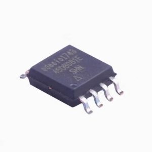
AT45DB081E-SHN-T
8Mbit DataFlash, dual-SPI 85MHz, 2x264B SRAM buffers, USON-8 (4x3mm), page-based ECC
Brand: Renesas
Package: USON-8 (4 x 3 x 0.6mm, 0.8mm pitch)
IN STOCK: 4500pcs
Cargo cycle: 3-7 Days
The minimum order is 1

PIC32MX795F512L-80I/PF
32-bit PIC32MX MCU with Ethernet/CAN/USB, 80MHz, 512KB Flash, TQFP-100, industrial
Brand: MICROCHIP
Package: TQFP-100 (14 x 14 mm)
IN STOCK: 7912pcs
Cargo cycle: 3-7 Days
The minimum order is 1