
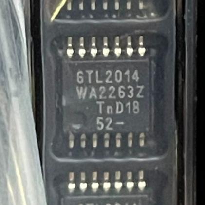





The GTL2014PW from NXP Semiconductors is a 4-bit LVTTL-to-GTL translating transceiver in a 14-pin TSSOP package (5.0 x 4.4 mm). It operates from a single 3.0 V to 3.6 V supply with 4 mA typical supply current. The LVTTL A-port inputs are 5.5 V tolerant, and the GTL B-port I/Os operate up to 3.6 V with open-drain outputs. A direction pin (DIR) configures the device as either a GTL-to-LVTTL sampling receiver or an LVTTL-to-GTL driver. VREF is adjustable from 0.5 V to VCC/2 for GTL threshold reference. The device supports partial power-down and provides ESD protection exceeding 2000 V HBM. Operating temperature range is -40°C to +85°C.
Home » Integrated Circuits ICs, Interface ICs » GTL2014PW
GTL2014PW
4-bit LVTTL-to-GTL transceiver, 3.0-3.6V, 5V-tolerant inputs, adjustable Vref, DIR pin, TSSOP-14, -40~85°C
3000
Effective Inventory
Manufacturer Part:
GTL2014PW
Package:
TSSOP-14 (SOT402-1) (5.0 x 4.4 x 1.1 mm, 0.65mm pitch)
Brand:
Product Categories:
Quality Commitment
Shipping & Payment
Service & Packaging
Product Manual
Other recommendations you may be interested in.
Description
Product Introduction: GTL2014PW Product Introduction
The GTL2014PW is a 4-bit translating transceiver from NXP designed to interface 3.3-V LVTTL logic with GTL (Gunning Transceiver Logic) buses commonly found in processor and memory controller applications. The device is pin-to-pin backward compatible with the GTL2005, with improved VREF tracking down to 0.5 V for low-voltage CPU interfaces.
GTL is an open-drain signaling standard that uses a reference voltage (VREF) to set the switching threshold. GTL signals swing between 0 V (low) and a termination voltage (VTT), typically 1.2 V or 1.5 V, with VREF at approximately VTT/2. This lower voltage swing compared to LVTTL enables faster edge rates and lower power dissipation at high frequencies, making GTL popular for processor front-side buses and high-speed memory interfaces.
The GTL2014 provides 4 bits of bidirectional level translation. When DIR is high, the device translates from LVTTL (A port) to GTL (B port) — the LVTTL inputs drive the GTL open-drain outputs. When DIR is low, the device translates from GTL (B port) to LVTTL (A port) — the GTL inputs are sampled against VREF and the results appear on the LVTTL outputs.
The A-port LVTTL inputs tolerate up to 5.5 V, allowing direct connection to 5-V CMOS or TTL logic. The B-port GTL I/Os are open-drain and tolerate up to 3.6 V, suitable for both standard GTL (VTT = 1.2 V) and GTL+ (VTT = 1.5 V) buses. The VREF pin accepts a reference voltage from 0.5 V to VCC/2 (1.8 V max at VCC = 3.6 V), accommodating modern low-voltage processors.
The GTL2014 is backward compatible with the GTL2005, though the A and B port labels are interchanged between the two devices. Designers migrating from GTL2005 should note this pin swap. The GTL2014’s improved VREF linearity below 0.8 V and slightly longer propagation delays distinguish it from the GTL2005.
Working Principle: GTL2014PW Working Principle
**GTL Signaling Interface:** GTL uses open-drain drivers with a resistive pull-up to VTT (typically 1.2 V or 1.5 V). The receiver compares the GTL bus voltage against VREF (approximately VTT/2) to determine the logic level. When the driver pulls the bus below VREF, the receiver detects a low. When the driver releases, the pull-up resistor pulls the bus above VREF, and the receiver detects a high.
**Direction Control (DIR Pin):** When DIR is high, the A-port LVTTL inputs drive the B-port GTL open-drain outputs. A high on an A-port input causes the corresponding B-port output to pull down (assert low on GTL bus); a low on the A-port input releases the B-port output (GTL bus pulled high by external termination). When DIR is low, the B-port GTL inputs are compared against VREF, and the results drive the A-port LVTTL push-pull outputs.
**VREF Reference:** The VREF pin establishes the switching threshold for the GTL receivers. It must be connected to a clean reference voltage, typically derived from VTT through a resistor divider. The GTL2014’s VREF tracks accurately down to 0.5 V, supporting low-voltage CPU cores.
**Partial Power-Down:** The I/O pins are designed to tolerate voltages when VCC is not applied, preventing backflow current damage in hot-swap and power-sequencing scenarios.
Pin Description: GTL2014PW Pin Definition and Functions
| Pin | Name | Type | Description |
|---|---|---|---|
| 1 | 1A | I/O | LVTTL I/O bit 0; 5.5V tolerant input; push-pull output when DIR=low (GTL-to-LVTTL) |
| 2 | 2A | I/O | LVTTL I/O bit 1; same characteristics as 1A |
| 3 | 3A | I/O | LVTTL I/O bit 2 |
| 4 | 4A | I/O | LVTTL I/O bit 3 |
| 5 | DIR | I | Direction control; HIGH = LVTTL-to-GTL (A drives B); LOW = GTL-to-LVTTL (B drives A); do not change while bus is active |
| 6 | GND | G | Ground |
| 7 | VREF | I | GTL reference voltage input; 0.5V to VCC/2; sets receiver threshold; connect to clean reference derived from VTT |
| 8 | 1B | I/O | GTL I/O bit 0; open-drain output; 3.6V tolerant; compared against VREF when receiving |
| 9 | 2B | I/O | GTL I/O bit 1 |
| 10 | 3B | I/O | GTL I/O bit 2 |
| 11 | 4B | I/O | GTL I/O bit 3 |
| 12-14 | GND/NC | G/- | Ground / no connect |
Application Scenarios: In which products and applications is GTL2014PW used
| Application | Description |
|---|---|
| Processor Front-Side Bus Interface | Connect 3.3V LVTTL chipset logic to GTL/GTL+ processor bus; DIR pin controlled by chipset; VREF set to VTT/2 (0.65V for GTL+); 4 bits cover address/data lines; use multiple devices for wider buses |
| Memory Controller GTL Bus | Translate between 3.3V memory controller and GTL-terminated DRAM bus; open-drain B-port drives GTL termination resistors; VREF derived from VTT supply; direction pin switches between read/write cycles |
Alternative Models: What chips are recommended as replacements for GTL2014PW
| Model | Manufacturer | Compatibility | Key Difference |
|---|---|---|---|
| GTL2005PW | NXP | Legacy Predecessor | 4-bit LVTTL-to-GTL transceiver; same TSSOP-14 footprint; A/B port labels swapped vs GTL2014; VREF degrades below 0.8V; shorter propagation delay; use only for legacy drop-in replacement |
| GTL2010PW | NXP | Series Variant (2-bit) | 2-bit LVTTL-to-GTL transceiver; smaller TSSOP-8 package; same electrical characteristics; use for narrower GTL buses |
| SN74GTL2014PWR | TI | Functional Equivalent | 4-bit LVTTL-to-GTL transceiver; TSSOP-14; similar specs; TI-sourced alternative; verify pinout compatibility before substituting |
Recommend Parts

ISL95855HRTZ-T
IMVP8 3+2+1 phase buck controller, R3 technology, 4.5-25V input, 48-TQFN
Brand: Renesas
Package: 48-TQFN (6×6 mm, exposed pad)
IN STOCK: 2156pcs
Cargo cycle: 3-7 Days
The minimum order is 1

IRFB4019PBF
150V N-Channel HEXFET Power MOSFET, 47A, 34 mΩ RDS(on), TO-220AB
Brand: infineon
Package: TO-220AB
IN STOCK: 2409pcs
Cargo cycle: 3-7 Days
The minimum order is 1

MSP430F247TPMR
TI MSP430 MCU, 16-bit RISC, 92KB Flash, 8KB RAM, 16MHz, LQFP-64
Brand: texas-instruments
Package: See datasheet
IN STOCK: 13371pcs
Cargo cycle: 3-7 Days
The minimum order is 1

UCC28740DR
CVCC Flyback Controller, 700V startup, opto feedback, <10mW no-load, SOIC-7
Brand: TI
Package: SOIC-7 (4.9 x 3.9 x 1.75 mm)
IN STOCK: 4840pcs
Cargo cycle: 3-7 Days
The minimum order is 1

MMUN2211LT1G
NPN digital transistor, R1=10kΩ R2=10kΩ, 50V, 100mA, SOT-23-3, pre-biased BRT switch
Brand: Onsemi
Package: SOT-23-3 (TO-236, SC-59)
IN STOCK: 8500pcs
Cargo cycle: 3-7 Days
The minimum order is 1

PIC32MX795F512L-80I/PF
32-bit PIC32MX MCU with Ethernet/CAN/USB, 80MHz, 512KB Flash, TQFP-100, industrial
Brand: MICROCHIP
Package: TQFP-100 (14 x 14 mm)
IN STOCK: 7912pcs
Cargo cycle: 3-7 Days
The minimum order is 1