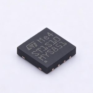
Opens in a new tab

KLM8G1GETF-B041

8GB eMMC 5.1, HS400, 153-ball FBGA, -25 to 85°C

2914

Effective Inventory

Image for reference only

Manufacturer Part:

KLM8G1GETF-B041

Package:

FBGA-153 (11.5 x 13 x 1.0 mm)

Brand:

Quality Commitment

Shipping & Payment

Service & Packaging

Product Manual

Description

The KLM8G1GETF-B041 by Samsung is an 8 GB eMMC 5.1 embedded flash storage device integrating 3D TLC NAND and an intelligent MMC controller in a FBGA-153 (11.5 x 13 x 1.0 mm) package. It supports HS400 mode for up to 330 MB/s sequential read and 50 MB/s sequential write over an 8-bit parallel MMC bus with data strobe. The integrated FTL handles wear leveling, bad block management, 40-bit/1KB ECC, and garbage collection transparently to the host.

Dual-voltage architecture: VCC 2.7-3.6V (NAND), VCCQ 1.7-1.95V or 2.7-3.6V (I/O). Partitions include User Area (~7.28 GiB), two 4 MB Boot Partitions, and 512 KB RPMB. Operating range -25 to +85C. RoHS compliant, ECCN 3A991.b.1.a. Mass Production. Ideal for industrial HMI, smart cameras, IoT gateways, and automotive infotainment.

Product Introduction: KLM8G1GETF-B041 Product Introduction

The KLM8G1GETF-B041 is an 8 GB embedded MultiMediaCard (eMMC) storage device manufactured by Samsung Electronics, compliant with the JEDEC eMMC 5.1 specification. It integrates 3D TLC NAND flash memory and an intelligent MMC controller in a single 153-ball FBGA package (11.5 x 13 x 1.0 mm), providing a complete managed NAND solution transparent to the host.

The device supports multiple speed modes including HS400 (200 MHz DDR with data strobe, up to 400 MB/s theoretical, 330 MB/s sequential read typical), HS200 (200 MHz SDR), High Speed (52 MHz), and Legacy mode. The 8-bit parallel data bus with CMD and CLK signals follows the standard MMC interface protocol, requiring no external NAND flash controller.

The dual-power architecture features VCC (2.7-3.6V for NAND array) and VCCQ (1.7-1.95V for 1.8V I/O mode or 2.7-3.6V for 3.3V I/O mode), allowing flexible host I/O voltage selection without level shifters. The integrated controller manages Flash Translation Layer (FTL) functions including dynamic wear leveling, bad block management, 40-bit/1KB ECC, and background garbage collection, all transparent to the host.

Storage partitions include a User Area (~7.28 GiB), two Boot Partitions (4 MB each for fast boot), and one RPMB partition (512 KB for anti-rollback security storage). The device supports eMMC health status monitoring via EXT_CSD registers (PRE_EOL_INFO, DEVICE_LIFE_TIME_EST). Sequential write speed is 50 MB/s typical. Operating temperature is -25 to +85C. RoHS compliant, ECCN 3A991.b.1.a. Product status: Mass Production.

Working Principle: KLM8G1GETF-B041 Working Principle

The KLM8G1GETF-B041 operates as a managed NAND flash storage device with the following architecture:

1. eMMC Protocol Interface: The host communicates via a standard MMC command set (CMD0-CMD62) over an 8-bit parallel data bus (DAT0-DAT7), a command line (CMD), and a clock line (CLK). In HS400 mode, an additional Data Strobe signal from the device synchronizes read data and CRC status, enabling DDR operation at 200 MHz for 400 MB/s bandwidth.

2. Integrated Flash Controller: The on-chip MMC controller manages all NAND flash operations transparently. It implements a Flash Translation Layer (FTL) that maps logical block addresses (LBAs) from the host to physical NAND pages, handling wear leveling, bad block remapping, ECC encoding/decoding, and garbage collection without host intervention.

3. NAND Flash Array: The internal 3D TLC (Triple-Level Cell) NAND stores 3 bits per cell for high density. The controller manages program/erase cycling and cell reliability through ECC (40-bit/1KB correction capability) and wear-leveling algorithms that distribute writes across the array to maximize endurance.

4. Partition Management: The device exposes three partition types. Boot Partitions (2 x 4 MB) support fast boot with configurable boot bus width and timing. The RPMB partition provides authenticated and replay-protected storage using HMAC-SHA256 for secure key and certificate storage. The User Area provides general-purpose storage accessible as a block device.

5. Dual Voltage Domains: VCC powers the NAND flash array at 3.3V, while VCCQ supplies the controller and I/O logic at either 1.8V or 3.3V, selected by the host. Independent power rails allow the host to power down VCC while maintaining VCCQ for low-power standby.

6. Speed Mode Negotiation: The device initializes in Legacy mode and the host negotiates higher speeds through EXT_CSD register writes. HS400 mode requires the host to first switch to HS200 (SDR), train timing, then switch to HS400 (DDR with strobe). The Data Strobe signal eliminates the need for host-side read data training.

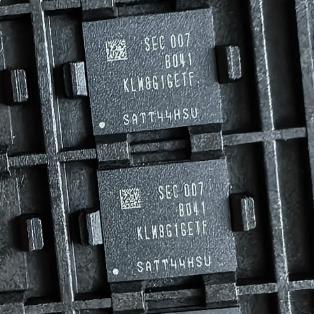
Pin Description: KLM8G1GETF-B041 Pin Definition and Functions
Pin Group Count Type Description
DAT0-DAT7 8 I/O Bidirectional 8-bit data bus for command response and data transfer
CMD 1 I/O Command/response line; open-drain for init, push-pull for data transfer
CLK 1 I Clock input from host (max 200 MHz in HS400 mode)
Data Strobe 1 O Output strobe for read data synchronization in HS400 DDR mode
RST_n 1 I Hardware reset (active low)
VCC 4 P NAND flash array power supply (2.7-3.6V)
VCCQ 5 P Controller and I/O power supply (1.7-1.95V or 2.7-3.6V)
VSS 11 G Ground connections
VDDI 1 P Internal regulator output (bypass with capacitor)
RFU Remaining – Reserved for future use (do not connect)
Application Scenarios: In which products and applications is KLM8G1GETF-B041 used
Application Description
Industrial HMI OS and application storage in industrial panel PCs and HMIs with HS400 bandwidth for fast boot and smooth UI
Smart Cameras Video clip buffering and firmware storage in IP cameras with managed NAND reliability for 24/7 operation
IoT Gateways Embedded Linux root filesystem storage with built-in wear leveling for reliable long-term field operation
Consumer Electronics Main storage in smart TVs, set-top boxes, and tablets with 330 MB/s read for responsive app loading
Automotive Infotainment Navigation maps, media storage, and firmware in vehicle head units with RPMB for secure boot authentication
Alternative Models: What chips are recommended as replacements for KLM8G1GETF-B041
Model Manufacturer Compatibility Key Difference
KLM4G1FETE-B041 Samsung Series Sibling 4 GB eMMC 5.1, smaller 11x10mm package, same protocol
KLMAG1JETD-B041 Samsung Series Sibling 16 GB eMMC 5.1, same FBGA-153 package, higher capacity
MTFC4GACAJCN-1M-WT Micron Competitive Alternative 4 GB eMMC 5.1, same FBGA-153 footprint, different manufacturer
THGBMJG6C1LBAB7 Kioxia (Toshiba) Competitive Alternative 8 GB eMMC 5.1, same package size, different controller
SDINBDG4-8G SanDisk/WD Competitive Alternative 8 GB eMMC 5.1, same package footprint, iNAND brand

Recommend Parts

ISL95855HRTZ-T

IMVP8 3+2+1 phase buck controller, R3 technology, 4.5-25V input, 48-TQFN

Brand: Renesas

Package: 48-TQFN (6×6 mm, exposed pad)

IN STOCK: 2156pcs

Cargo cycle: 3-7 Days

The minimum order is 1

IRFB4019PBF

150V N-Channel HEXFET Power MOSFET, 47A, 34 mΩ RDS(on), TO-220AB

Brand: infineon

Package: TO-220AB

IN STOCK: 2409pcs

Cargo cycle: 3-7 Days

The minimum order is 1

MSP430F247TPMR

TI MSP430 MCU, 16-bit RISC, 92KB Flash, 8KB RAM, 16MHz, LQFP-64

Package: See datasheet

IN STOCK: 13371pcs

Cargo cycle: 3-7 Days

The minimum order is 1

UCC28740DR

CVCC Flyback Controller, 700V startup, opto feedback, <10mW no-load, SOIC-7

Brand: TI

Package: SOIC-7 (4.9 x 3.9 x 1.75 mm)

IN STOCK: 4840pcs

Cargo cycle: 3-7 Days

The minimum order is 1

MMUN2211LT1G

NPN digital transistor, R1=10kΩ R2=10kΩ, 50V, 100mA, SOT-23-3, pre-biased BRT switch

Brand: Onsemi

Package: SOT-23-3 (TO-236, SC-59)

IN STOCK: 8500pcs

Cargo cycle: 3-7 Days

The minimum order is 1

PIC32MX795F512L-80I/PF

32-bit PIC32MX MCU with Ethernet/CAN/USB, 80MHz, 512KB Flash, TQFP-100, industrial

Brand: MICROCHIP

Package: TQFP-100 (14 x 14 mm)

IN STOCK: 7912pcs

Cargo cycle: 3-7 Days

The minimum order is 1