
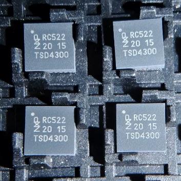





The MFRC52202HN1 from NXP Semiconductors is the version 2.0 of the MFRC522 highly integrated reader/writer IC for contactless communication at 13.56 MHz, in an HVQFN-32 (5x5x0.85mm) package. It supports ISO/IEC 14443A/MIFARE and NTAG protocols with data rates up to 848 kBd. The internal transmitter directly drives an antenna via TX1/TX2 outputs without additional active circuitry, while the receiver provides robust demodulation and decoding. The digital module handles complete ISO/IEC 14443A framing, parity, and CRC error detection. Host interfaces: SPI (up to 10 Mbit/s), I2C (up to 400 kHz), and serial UART. A 64-byte FIFO buffer handles data transfer. Features include MIFARE Classic encryption support, MFIN/MFOUT for secure module communication, programmable timer, flexible interrupt modes, and hardware power-down. Supply voltage: 2.5V to 3.6V. Current consumption: 5uA in power-down, 7mA typical active. Operating temperature: -25C to 85C. Version 2.0 adds an additional timer prescaler and corrected CRC handling with RX Multiple. RoHS, EAR99.
Home » Integrated Circuits ICs, Interface ICs » MFRC52202HN1
MFRC52202HN1
13.56MHz RFID reader/writer IC, ISO 14443A/MIFARE/NTAG, SPI/I2C/UART, HVQFN-32, ver2.0, -25~85C
Effective Inventory
Manufacturer Part:
MFRC52202HN1
Package:
HVQFN-32 (SOT617-1) (5 x 5 x 0.85 mm)
Brand:
Product Categories:
Quality Commitment
Shipping & Payment
Service & Packaging
Product Manual
Other recommendations you may be interested in.
Description
Product Introduction: MFRC52202HN1 Product Introduction
The MFRC52202HN1 from NXP Semiconductors is the version 2.0 of the MFRC522 highly integrated reader/writer IC for contactless communication at 13.56 MHz, housed in a compact HVQFN-32 package (5 x 5 x 0.85 mm, SOT617-1). This device is one of the most widely used RFID reader ICs in the embedded systems community, supporting ISO/IEC 14443A/MIFARE and NTAG protocols for reading and writing contactless cards and transponders.
The MFRC52202HN1 integrates the complete analog front end (AFE), digital protocol processing, and host communication interfaces into a single chip. The internal transmitter provides buffered output drivers (TX1, TX2) that can directly drive a reader/writer antenna matched to 50 ohms with minimal external components. The receiver module includes a robust and efficient implementation for demodulating and decoding signals from ISO/IEC 14443A/MIFARE compatible cards, with a typical operating distance of up to 50 mm depending on antenna design and tuning.
The digital module manages the complete ISO/IEC 14443A framing and error detection (parity and CRC) functionality, along with MIFARE Classic authentication (CRYPTO1 encryption for MF1xxS20, MF1xxS50, MF1xxS70 in Read/Write mode). A 64-byte FIFO buffer facilitates efficient data transfer between the host and the contactless UART. The device supports three host communication interfaces: SPI (up to 10 Mbit/s), I2C (up to 400 kHz, 7-bit address programmable via EA pin and D1-D5), and serial UART (up to 1.2 Mbit/s), selectable by pin configuration.
Version 2.0 improvements over version 1.0 (MFRC52201HN1) include: increased stability in rough conditions, an additional timer prescaler for more flexible timing configurations, and corrected CRC handling when RX Multiple is set to 1. The MFRC52202HN1 is fully backward compatible with the MFRC52201HN1.
Power management features include a hardware power-down mode (via NRSTPD pin) with 5uA typical current consumption, and a software-controlled power-down mode with programmable timer for automatic wake-up. The device operates from a 2.5V to 3.6V supply, making it suitable for 3.3V microcontroller systems. The operating temperature range is -25C to 85C.
The HN1 suffix denotes HVQFN-32 package, and the ordering codes include ,151 and ,157 variants for different packaging options (tape and reel). The device is RoHS compliant, MSL Level 1, and classified as EAR99.
Working Principle: MFRC52202HN1 Working Principle
The MFRC52202HN1 operates as a 13.56 MHz RFID reader/writer, implementing the physical and data link layers of the ISO/IEC 14443A communication protocol between a host microcontroller and contactless cards or transponders.
Transmitter Operation: The internal transmitter generates the 13.56 MHz carrier frequency using an external 27.12 MHz crystal oscillator (connected to OSCIN/OSCOUT pins) with an internal PLL. The carrier is modulated using either 100% ASK (Type A modification) or various modulation depths as configured in the TxControlReg register. The modulated carrier is driven through two push-pull output stages (TX1 and TX2) that connect to the antenna via an LC matching network. When both TX1 and TX2 are enabled (TxControlReg bits 0 and 1 set), the outputs drive the antenna in push-pull configuration for maximum power delivery. The transmitter supports ISO/IEC 14443A transfer speeds: 106 kBd, 212 kBd, 424 kBd, and 848 kBd.
Receiver Operation: The receiver input (RX pin) captures the subcarrier signal from the card’s load modulation. The signal passes through a gain-controlled amplifier, then through I-channel and Q-channel demodulators using coherent detection with internally generated reference signals. The demodulated signals are digitized by an ADC and processed by the digital correlator for bit decoding. The receiver handles the complete ISO/IEC 14443A receive chain including bit-level framing, anti-collision protocol, and collision detection. The collision detection identifies bit positions where multiple cards transmit different values simultaneously.
Protocol Processing: The digital module (contactless UART) manages the complete ISO/IEC 14443A protocol stack: (1) REQA/WUPA command transmission for card activation, (2) Anti-collision sequence to select one card from multiple cards in the field, (3) SELECT command to confirm card selection, (4) MIFARE authentication (CRYPTO1 mutual authentication using secret key), (5) Read/Write operations with automatic CRC generation and verification. The 64-byte FIFO buffer stores transmitted and received data, allowing the host to read/write large data blocks without tight timing requirements.
Host Interface Selection: The interface mode is determined at power-up by the state of the I2C pin (pin 1) and the D1-D7 pins. When I2C pin is HIGH, the I2C interface is selected with the 7-bit slave address determined by the EA pin and D1-D5 pins. When I2C pin is LOW, either SPI or UART mode is selected based on pin configurations. In SPI mode, the device uses standard 4-wire SPI (NSS, SCK, MOSI, MISO) with NSS active-low chip select. In UART mode, the device uses serial communication with configurable baud rate.
MIFARE Authentication: The MFRC52202HN1 implements the CRYPTO1 stream cipher for MIFARE Classic authentication. During the authentication sequence, the reader sends an authentication command with the sector and key type (A or B), the card responds with a random number, and the reader and card perform a mutual three-pass authentication. After successful authentication, all subsequent read/write operations in that sector are encrypted using the CRYPTO1 cipher. The MFIN and MFOUT pins allow connection to a secure access module (SAM) for enhanced key management.
Interrupt System: The IRQ pin generates interrupts for various events including: timer expiration, end of transmit, receiver FIFO full/half-full/break, CRC error, and collision detection. The interrupt enable and status registers allow fine-grained control over which events trigger interrupts, enabling event-driven programming models that reduce host processor polling overhead.
Pin Description: MFRC52202HN1 Pin Definition and Functions
| Pin | Name | Type | Description |
|---|---|---|---|
| 1 | I2C | Input | I2C interface enable; HIGH selects I2C mode; LOW selects SPI or UART mode based on D7-D5 pin states; must be tied at power-up |
| 2 | PVDD | Power | Pad power supply; 2.5V to 3.6V; powers the I/O pad ring |
| 3 | DVDD | Power | Digital power supply; 2.5V to 3.6V; powers the digital core; connect 100nF decoupling capacitor to DVSS |
| 4 | DVSS | Ground | Digital ground |
| 5 | PVSS | Ground | Pad power supply ground |
| 6 | NRSTPD | Input | Not Reset and Power-down; LOW enters hard power-down (oscillator inhibited, inputs disconnected); rising edge triggers internal reset; must be HIGH for normal operation |
| 7 | MFIN | Input | MIFARE signal input; receives serial data from a secure access module (SAM) or external MIFARE module |
| 8 | MFOUT | Output | MIFARE signal output; sends serial data to a SAM or external module; provides internal power supply to connected smart card IC via MFIN/MFOUT |
| 9 | SVDD | Power | MFIN/MFOUT pad power supply; powers the MFIN and MFOUT pin circuits |
| 10 | TVSS | Ground | Transmitter output stage ground (for TX1) |
| 11 | TX1 | Output | Transmitter output 1; delivers the modulated 13.56 MHz energy carrier to antenna; push-pull output; controlled by TxControlReg |
| 12 | TVDD | Power | Transmitter power supply; 2.5V to 3.6V; supplies both TX1 and TX2 output stages; requires low-ESR decoupling |
| 13 | TX2 | Output | Transmitter output 2; second 13.56 MHz carrier output for push-pull antenna driving; push-pull output; controlled by TxControlReg |
| 14 | TVSS | Ground | Transmitter output stage ground (for TX2) |
| 15 | AVDD | Power | Analog power supply; 2.5V to 3.6V; powers the analog receiver section; critical for RX sensitivity; requires clean supply |
| 16 | VMID | Power | Internal reference voltage output; connect 100nF capacitor to AVSS for stability; provides internal analog reference |
| 17 | RX | Input | Receiver input; receives the subcarrier signal from the antenna via external conditioning circuitry; AC-coupled recommended |
| 18 | AVSS | Ground | Analog ground; connect to system ground plane |
| 19 | AUX1 | Output | Auxiliary output 1; used for test and diagnostic purposes; can be configured to output internal analog signals |
| 20 | AUX2 | Output | Auxiliary output 2; test output; can monitor internal PLL and demodulator signals |
| 21 | OSCIN | Input | Crystal oscillator input; connects to 27.12 MHz crystal or external clock source; requires load capacitors |
| 22 | OSCOUT | Output | Crystal oscillator output; connects to 27.12 MHz crystal; leave open if using external clock on OSCIN |
| 23 | IRQ | Output | Interrupt request output; active LOW; signals various events (timer, TX complete, RX ready, CRC error, collision); open-drain with internal pullup |
| 24 | SDA/NSS/RX | I/O | Multi-function pin: I2C SDA (I2C mode), SPI NSS chip select (SPI mode), UART RX receive (UART mode) |
| 25 | D1/ADR_5 | I/O | Data pin 1 / I2C address bit 5; SPI: D1 data; I2C: ADR_5 address bit; UART: data |
| 26 | D2/ADR_4 | I/O | Data pin 2 / I2C address bit 4 |
| 27 | D3/ADR_3 | I/O | Data pin 3 / I2C address bit 3 |
| 28 | D4/ADR_2 | I/O | Data pin 4 / I2C address bit 2 |
| 29 | D5/ADR_1/SCK/DTRQ | I/O | Multi-function: D5 data / ADR_1 address / SPI SCK clock / UART DTRQ data terminal ready |
| 30 | D6/ADR_0/MOSI/MX | I/O | Multi-function: D6 data / ADR_0 address / SPI MOSI master-out / UART MX mixed data |
| 31 | D7/SCL/MISO/TX | I/O | Multi-function: D7 data / I2C SCL clock / SPI MISO master-in / UART TX transmit |
| 32 | EA | Input | External address; used for coding I2C address; tied HIGH or LOW to set the MSB of the I2C slave address |
Application Scenarios: In which products and applications is MFRC52202HN1 used
| Application | Description |
|---|---|
| Access Control Systems | Door entry and building security using MIFARE cards; anti-collision supports multiple cards in the field; CRYPTO1 authentication prevents card cloning; typical read distance 50mm |
| Public Transportation Ticketing | Contactless fare collection using MIFARE Ultralight or Classic cards; 848 kBd high-speed mode enables fast throughput at turnstiles; NTAG support for modern ticketing |
| Embedded RFID Modules | Widely used in Arduino and embedded development boards (RFID-RC522 module); SPI interface at 10 Mbit/s for fast register access; extensive open-source driver ecosystem |
| Electronic Payment Terminals | Contactless payment using ISO/IEC 14443A cards; MFIN/MFOUT interface connects to secure access module (SAM) for key management and transaction security |
| Library and Asset Management | NTAG-based item tracking; 64-byte FIFO enables efficient bulk read/write of NDEF messages; low power-down current (5uA) extends battery life in portable readers |
Alternative Models: What chips are recommended as replacements for MFRC52202HN1
| Model | Manufacturer | Compatibility | Key Difference |
|---|---|---|---|
| MFRC52201HN1 | NXP | Predecessor Version | Version 1.0; same pinout and package; missing additional timer prescaler and CRC fix; fully compatible register map; version 2.0 recommended for new designs |
| CLRC66302HN | NXP | Upgraded Replacement | Next-generation RFID/NFC frontend; supports more protocols (ISO 14443A/B, FeliCa, NFC); higher output power; different register map; requires software migration |
| PN5321A3HN | NXP | Functionally Similar | NFC controller with card emulation and peer-to-peer; more features but different architecture; not a drop-in replacement; larger package |
| MFRC522B | JSMSEMI | Pin-Compatible Clone | Third-party compatible version; QFN-32-EP (5×5); same register map and firmware; verify performance for critical applications |
| CR95HF | ST | Functionally Similar | 13.56 MHz multi-protocol transceiver; ISO 14443A/B and 15693; SPI/UART interface; no I2C; different register map and command set |
Recommend Parts

ISL95855HRTZ-T
IMVP8 3+2+1 phase buck controller, R3 technology, 4.5-25V input, 48-TQFN
Brand: Renesas
Package: 48-TQFN (6×6 mm, exposed pad)
IN STOCK: 2156pcs
Cargo cycle: 3-7 Days
The minimum order is 1

IRFB4019PBF
150V N-Channel HEXFET Power MOSFET, 47A, 34 mΩ RDS(on), TO-220AB
Brand: infineon
Package: TO-220AB
IN STOCK: 2409pcs
Cargo cycle: 3-7 Days
The minimum order is 1

MSP430F247TPMR
TI MSP430 MCU, 16-bit RISC, 92KB Flash, 8KB RAM, 16MHz, LQFP-64
Brand: texas-instruments
Package: See datasheet
IN STOCK: 13371pcs
Cargo cycle: 3-7 Days
The minimum order is 1

UCC28740DR
CVCC Flyback Controller, 700V startup, opto feedback, <10mW no-load, SOIC-7
Brand: TI
Package: SOIC-7 (4.9 x 3.9 x 1.75 mm)
IN STOCK: 4840pcs
Cargo cycle: 3-7 Days
The minimum order is 1

MMUN2211LT1G
NPN digital transistor, R1=10kΩ R2=10kΩ, 50V, 100mA, SOT-23-3, pre-biased BRT switch
Brand: Onsemi
Package: SOT-23-3 (TO-236, SC-59)
IN STOCK: 8500pcs
Cargo cycle: 3-7 Days
The minimum order is 1

PIC32MX795F512L-80I/PF
32-bit PIC32MX MCU with Ethernet/CAN/USB, 80MHz, 512KB Flash, TQFP-100, industrial
Brand: MICROCHIP
Package: TQFP-100 (14 x 14 mm)
IN STOCK: 7912pcs
Cargo cycle: 3-7 Days
The minimum order is 1