Opens in a new tab

TPS5430DDAR

3A, 36V step-down DC-DC converter, 500 kHz, SO PowerPAD-8

5321

Effective Inventory

Image for reference only

Manufacturer Part:

TPS5430DDAR

Package:

8-SO PowerPAD (HSOIC-8, 5 x 4 x 1.55 mm)

Brand:

Quality Commitment

Shipping & Payment

Service & Packaging

Product Manual

Description

The TPS5430DDAR by Texas Instruments is a 3A step-down DC-DC converter with a wide 5.5V to 36V input range and adjustable output from 1.22V to 31V. It integrates a 100 mOhm high-side MOSFET for up to 95% efficiency, with a fixed 500 kHz switching frequency enabling small external filter components. Internal compensation eliminates external loop components, and input voltage feedforward ensures stable transient response across the full input range.

Protection features include cycle-by-cycle current limiting, overvoltage protection, UVLO, and thermal shutdown. The ENA pin provides on/off control (15 uA shutdown Iq), and internal slow start (8 ms) limits inrush current. Packaged in 8-SO PowerPAD (HSOIC-8) with exposed thermal pad, operating from -40 to +125C junction. MSL-2, lead-free, RoHS/REACH compliant. ECCN EAR99. Active. Ideal for 24V industrial bus conversion, automotive power, and embedded supplies.

Product Introduction: TPS5430DDAR Product Introduction

The TPS5430DDAR is a 3A step-down (buck) DC-DC converter manufactured by Texas Instruments, part of the SWIFT family. It features a wide input voltage range of 5.5V to 36V with an adjustable output voltage from 1.22V to 31V, set via an external resistor divider with 1.5% initial reference accuracy. The device integrates a 100 mOhm high-side N-channel MOSFET switch, achieving up to 95% efficiency.

The fixed 500 kHz switching frequency enables use of small external inductors and capacitors, minimizing solution footprint. Internal compensation simplifies design by eliminating external compensation network components. An input voltage feedforward circuit improves line regulation and transient response across the wide input range.

Key protection features include cycle-by-cycle overcurrent limiting, output overvoltage protection via a fast OVP comparator, undervoltage lockout (UVLO) that prevents operation below 5.5V input, and thermal shutdown. An active-high ENA (enable) pin with internal pull-up allows on/off control; pulling ENA below 0.5V disables the device and reduces quiescent current to 15 uA typical.

The internal slow-start circuit ramps the output voltage over 8 ms typical, limiting inrush current and preventing output overshoot during startup. A BOOT pin requires an external 0.01 uF bootstrap capacitor between BOOT and PH (phase node) to drive the high-side MOSFET gate.

The device is packaged in a thermally enhanced 8-pin SO PowerPAD (DDA) package with an exposed thermal pad for efficient heat dissipation. Operating junction temperature range is -40 to +125C. MSL-2 (260C, 1 year). Lead-free (NiPdAu finish), RoHS compliant, REACH compliant. ECCN: EAR99. Product status: Active.

Working Principle: TPS5430DDAR Working Principle

The TPS5430DDAR operates as a current-mode PWM buck converter with the following subsystem architecture:

1. Power Stage: The integrated 100 mOhm N-channel MOSFET switches the input voltage to the output inductor at 500 kHz. During the on-time, current flows from VIN through the MOSFET, through the output inductor to the load, and returns through GND. During the off-time, the inductor current freewheels through the external Schottky catch diode. The 500 kHz fixed frequency is set by an internal oscillator, and the duty cycle is modulated by the feedback loop.

2. Voltage Mode Control with Feedforward: The error amplifier compares the VSENSE pin voltage (from the output resistor divider) against the 1.221V internal reference. The error signal controls the PWM comparator, which determines the MOSFET on-time. Input voltage feedforward adjusts the PWM ramp slope proportionally to VIN, maintaining constant loop gain and improving line transient response across the wide 5.5-36V input range.

3. Internal Compensation: The feedback loop is internally compensated with a Type III network, eliminating external compensation components. This simplifies design but constrains the allowable output inductor and capacitor values to maintain stability (typically 10-22 uH inductor and 100-440 uF output capacitor).

4. Bootstrap Gate Drive: The BOOT pin provides gate drive voltage for the high-side MOSFET. An external 0.01 uF capacitor between BOOT and PH is charged during the off-time when PH is near ground. During the on-time, the BOOT capacitor provides the voltage above VIN needed to drive the N-channel MOSFET gate.

5. Protection Mechanisms: Cycle-by-cycle current limiting protects the MOSFET by terminating the on-time when the peak inductor current exceeds the limit. Overvoltage protection (OVP) turns off the MOSFET when VSENSE exceeds 112.5% of the reference. UVLO holds the device in reset until VIN exceeds the start threshold. Thermal shutdown disables switching when junction temperature exceeds the threshold.

6. Enable and Slow Start: The ENA pin provides on/off control. When enabled, the internal slow-start circuit ramps the reference from 0V to 1.221V over 8 ms, limiting inrush current. The slow-start also prevents output overshoot after fault recovery.

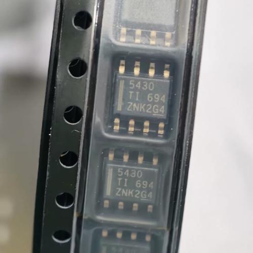
Pin Description: TPS5430DDAR Pin Definition and Functions
Pin Name Type Description
1 BOOT P Bootstrap capacitor connection for high-side MOSFET gate drive; connect 0.01 uF cap to PH
2 VCC I Internal regulator output bypass; connect 0.1 uF cap to GND (do not load externally)
3 VSENSE I Output voltage feedback input; connect to output resistor divider center tap
4 ENA I Enable control; float = ON (internal pull-up), LOW (<0.5V) = shutdown (15 uA Iq)
5 VIN P Input power supply (5.5V to 36V); bypass to GND with ceramic capacitor
6 PH O Phase node (switch output); connect to output inductor and catch diode
7 GND G Ground (signal and power); connect to PowerPAD thermal pad
8 GND G Ground (signal and power); connect to PowerPAD thermal pad
Pad PowerPAD G Exposed thermal pad; connect to PCB ground plane for heat dissipation
Application Scenarios: In which products and applications is TPS5430DDAR used
Application Description
24V Industrial Bus Step-down 24V industrial bus to 5V or 3.3V logic rails in PLCs, motor drives, and factory automation equipment
Automotive Systems Convert 12V battery to 5V/3.3V in body electronics and infotainment; wide input range accommodates load dump transients
Embedded Power Supplies Generate 3.3V or 5V from 12V/24V input for MCU and FPGA boards with 95% efficiency minimizing thermal design
Battery-Powered Devices High efficiency conversion from 6-24V battery packs to system rails in portable test equipment and instrumentation
Distributed Power Architectures Intermediate bus conversion from 48V/24V to point-of-load input range in telecom and networking equipment
Alternative Models: What chips are recommended as replacements for TPS5430DDAR
Model Manufacturer Compatibility Key Difference
TPS5431DDAR TI Series Sibling Same device with 23V max input (vs 36V); use when lower VIN range is acceptable
LM2596T-5.0 TI Competitive Alternative 3A buck, 4-40V input, 150 kHz (lower freq, larger inductor), TO-263 package
AP64352SP-13 Diodes Inc Competitive Alternative 3.5A buck, 4.5-36V input, 500 kHz, SO-8EP package, similar performance
MAX5035DASA+ Maxim/Analog Competitive Alternative 1A buck, 7.6-76V input, 125 kHz, higher voltage range but lower current
TPS5450DDAR TI Series Upgrade 5A output version of TPS5430, same package and pinout, higher current capability

Recommend Parts

ISL95855HRTZ-T

IMVP8 3+2+1 phase buck controller, R3 technology, 4.5-25V input, 48-TQFN

Brand: Renesas

Package: 48-TQFN (6×6 mm, exposed pad)

IN STOCK: 2156pcs

Cargo cycle: 3-7 Days

The minimum order is 1

IRFB4019PBF

150V N-Channel HEXFET Power MOSFET, 47A, 34 mΩ RDS(on), TO-220AB

Brand: infineon

Package: TO-220AB

IN STOCK: 2409pcs

Cargo cycle: 3-7 Days

The minimum order is 1

MSP430F247TPMR

TI MSP430 MCU, 16-bit RISC, 92KB Flash, 8KB RAM, 16MHz, LQFP-64

Package: See datasheet

IN STOCK: 13371pcs

Cargo cycle: 3-7 Days

The minimum order is 1

UCC28740DR

CVCC Flyback Controller, 700V startup, opto feedback, <10mW no-load, SOIC-7

Brand: TI

Package: SOIC-7 (4.9 x 3.9 x 1.75 mm)

IN STOCK: 4840pcs

Cargo cycle: 3-7 Days

The minimum order is 1

MMUN2211LT1G

NPN digital transistor, R1=10kΩ R2=10kΩ, 50V, 100mA, SOT-23-3, pre-biased BRT switch

Brand: Onsemi

Package: SOT-23-3 (TO-236, SC-59)

IN STOCK: 8500pcs

Cargo cycle: 3-7 Days

The minimum order is 1

PIC32MX795F512L-80I/PF

32-bit PIC32MX MCU with Ethernet/CAN/USB, 80MHz, 512KB Flash, TQFP-100, industrial

Brand: MICROCHIP

Package: TQFP-100 (14 x 14 mm)

IN STOCK: 7912pcs

Cargo cycle: 3-7 Days

The minimum order is 1