
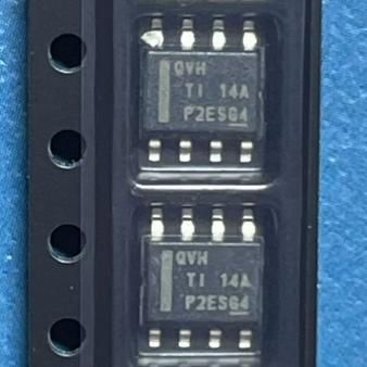


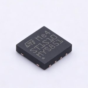



The TPS7A7001DDAR from Texas Instruments is a 2-A adjustable ultra-low-dropout (LDO) voltage regulator in an 8-pin HSOIC PowerPAD package (4.9 x 6.0 mm). It operates with input voltage as low as 1.425 V up to 6.5 V, with adjustable output from 0.5 V to 5 V set via external resistor divider. Maximum dropout is 380 mV at 2 A. The device features an enable pin with 1-µA shutdown quiescent current, 200 mV typical dropout at 1 A, 2% output accuracy, current limit and thermal shutdown protection. PSRR is 28 dB at 100 kHz. Operating temperature range is -40°C to +125°C. Target applications include telecom and networking cards, motherboard peripherals, set-top boxes, and battery-powered systems requiring very low VIN-to-VOUT differential at high current.
Home » Integrated Circuits ICs, Low Dropout Regulators (LDO) » TPS7A7001DDAR
TPS7A7001DDAR
2A adjustable LDO, 1.425-6.5V in, 0.5-5V out, 200mV Vdo@1A, enable pin, HSOIC-8 PowerPAD, -40~125°C
Effective Inventory
Manufacturer Part:
TPS7A7001DDAR
Package:
HSOIC-8 PowerPAD (DDA) (4.9 x 6.0 x 1.55 mm, 1.27mm pitch, exposed thermal pad)
Brand:
Product Categories:
Quality Commitment
Shipping & Payment
Service & Packaging
Product Manual
Other recommendations you may be interested in.
Description
Product Introduction: TPS7A7001DDAR Product Introduction
The TPS7A7001 is a high-performance positive-voltage LDO regulator from TI designed for applications requiring very low input voltage and very low dropout at up to 2 A. The device operates with input voltage as low as 1.425 V, making it suitable for low-voltage rails derived from single-cell Li-ion or point-of-load converters. The output voltage is adjustable from 0.5 V using an external resistor divider, with a 0.5-V internal reference.
The ultra-low dropout voltage (200 mV typical at 1 A, 380 mV max at 2 A) enables efficient regulation where VOUT is close to VIN, minimizing power dissipation. The enable (EN) pin provides on/off control with only 1-µA quiescent current in shutdown, suitable for power-sequencing and standby modes.
The HSOIC-8 PowerPAD package (DDA) provides a low thermal resistance of 46.4°C/W junction-to-ambient when soldered to a PCB with thermal vias. This allows the device to dissipate up to 2 W in typical PCB configurations without overheating, sufficient for 2-A loads with up to 1 V of input-to-output differential.
The internal current limit and thermal shutdown protect the device during fault conditions. The 2% output accuracy over line, load, and temperature ensures stable supply rails for sensitive loads such as FPGAs, DSPs, and RF sections. The minimum 4.7-µF output capacitor (ceramic) ensures stability with low ESR.
The TPS7A7001 complements TI’s lower-current LDO families (TPS736xx, TPS737xx) by providing higher output current while maintaining low dropout, filling the gap between 1-A LDOs and switching regulators for mid-power POL applications.
Working Principle: TPS7A7001DDAR Working Principle
**Pass Transistor Regulation:** The TPS7A7001 uses a P-channel MOSFET pass transistor driven by an error amplifier. The error amplifier compares a fraction of the output voltage (via the external R1/R2 divider) with the internal 0.5-V bandgap reference. When VOUT drops below the target, the error amplifier drives the PMOS gate harder, reducing RDS(on) and increasing output current. When VOUT rises above the target, the gate drive reduces, increasing RDS(on) and decreasing output current.
**Dropout Operation:** In dropout, the PMOS pass transistor is fully enhanced (gate driven to near ground). The dropout voltage equals ID x RDS(on) of the fully-enhanced PMOS. The low 200-mV dropout at 1 A reflects the low channel resistance of the large PMOS device.
**Enable and Shutdown:** The EN pin controls an internal bias circuit. When EN is below the threshold (~1.2 V), all internal bias is disabled, and the output is high-impedance. Ground current drops to 1 µA maximum. When EN is above the threshold, the regulator operates normally.
**Protection Circuits:** The current limit circuit senses output current and clamps it to a safe level (typically 2.8 A) during overload. The thermal shutdown disables the output when junction temperature exceeds ~160°C, with ~20°C hysteresis to prevent oscillation.
Pin Description: TPS7A7001DDAR Pin Definition and Functions
| Pin | Name | Type | Description |
|---|---|---|---|
| 1 | NC | – | No internal connection; leave floating or connect to GND |
| 2 | EN | I | Enable input; drive high (>1.2V) to enable regulator; drive low (<0.4V) to enter shutdown (1µA IQ); do not leave floating |
| 3 | NC | – | No internal connection |
| 4 | IN | P | Input supply; 1.425V to 6.5V; bypass with ≥4.7µF ceramic capacitor to GND |
| 5 | OUT | O | Regulated output; connect external R1/R2 divider to FB; bypass with ≥4.7µF ceramic; max load 2A |
| 6 | FB | I | Feedback input; connect to R1/R2 divider junction; VFB = 0.5V reference; output voltage = 0.5V x (1 + R1/R2) |
| 7 | GND | G | Ground; connect to PCB ground plane |
| 8 | NC | – | No internal connection |
| Pad | PowerPAD | G | Exposed thermal pad; electrically GND; solder to PCB ground plane with thermal vias for heat dissipation |
Application Scenarios: In which products and applications is TPS7A7001DDAR used
| Application | Description |
|---|---|
| Low-Voltage POL Regulator | Regulate 1.8V/2.5V rail to 1.0-1.5V at 1-2A for FPGA/DSP core; VIN as low as 1.425V enables direct regulation from 1.8V bus; 200mV dropout leaves 300mV headroom; pair with sequencing controller for power-up ordering |
| Li-Ion Battery Powered System | Regulate 3.6-4.2V battery to 3.3V at up to 2A; dropout <200mV at 1A allows operation down to 3.5V battery; enable pin for load switching; 1µA shutdown extends battery life in sleep mode |
| Telecom Line Card | Regulate 3.3V or 5V intermediate rail to lower voltage for ASIC/PHY; enable pin supports hot-swap sequencing; thermal shutdown protects during fault; SO-8 PowerPAD fits dense line cards |
Alternative Models: What chips are recommended as replacements for TPS7A7001DDAR
| Model | Manufacturer | Compatibility | Key Difference |
|---|---|---|---|
| TPS7A7002DDAR | TI | Series Variant | Same 2A LDO in DDA package; fixed output voltage options; no external resistors needed; use when fixed output preferred |
| TLV75501PDRV | TI | Functional Equivalent | 1A adjustable LDO; 2.0-5.5V input; 160mV dropout@1A; SOT-23-6; lower current but smaller footprint; use for <1A loads |
| NCV8164AMX330TCG | onsemi | Competitive Alternative | 300mA LDO; 2.2-5.5V; ultra-low noise; automotive AEC-Q100; use for automotive low-noise applications at lower current |
| AP2112K-ADJTRG1 | Diodes Inc | Functional Equivalent | 600mA adjustable LDO; 2.5-6V input; SOT-23-5; much lower current; use for light-load low-cost applications |
Recommend Parts

ISL95855HRTZ-T
IMVP8 3+2+1 phase buck controller, R3 technology, 4.5-25V input, 48-TQFN
Brand: Renesas
Package: 48-TQFN (6×6 mm, exposed pad)
IN STOCK: 2156pcs
Cargo cycle: 3-7 Days
The minimum order is 1

IRFB4019PBF
150V N-Channel HEXFET Power MOSFET, 47A, 34 mΩ RDS(on), TO-220AB
Brand: infineon
Package: TO-220AB
IN STOCK: 2409pcs
Cargo cycle: 3-7 Days
The minimum order is 1

MSP430F247TPMR
TI MSP430 MCU, 16-bit RISC, 92KB Flash, 8KB RAM, 16MHz, LQFP-64
Brand: texas-instruments
Package: See datasheet
IN STOCK: 13371pcs
Cargo cycle: 3-7 Days
The minimum order is 1

UCC28740DR
CVCC Flyback Controller, 700V startup, opto feedback, <10mW no-load, SOIC-7
Brand: TI
Package: SOIC-7 (4.9 x 3.9 x 1.75 mm)
IN STOCK: 4840pcs
Cargo cycle: 3-7 Days
The minimum order is 1

MMUN2211LT1G
NPN digital transistor, R1=10kΩ R2=10kΩ, 50V, 100mA, SOT-23-3, pre-biased BRT switch
Brand: Onsemi
Package: SOT-23-3 (TO-236, SC-59)
IN STOCK: 8500pcs
Cargo cycle: 3-7 Days
The minimum order is 1

PIC32MX795F512L-80I/PF
32-bit PIC32MX MCU with Ethernet/CAN/USB, 80MHz, 512KB Flash, TQFP-100, industrial
Brand: MICROCHIP
Package: TQFP-100 (14 x 14 mm)
IN STOCK: 7912pcs
Cargo cycle: 3-7 Days
The minimum order is 1