



Opens in a new tab

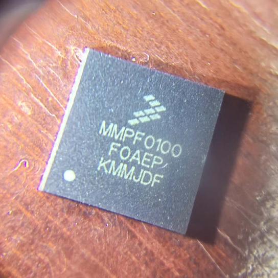
MMPF0100F0AEP

14-channel configurable PMIC, 6 buck + 7 LDO + boost, F0 OTP pre-programmed for i.MX 6Q/D, 4.5 A max, HVQFN-56

5183

Effective Inventory

Image for reference only

Manufacturer Part:

MMPF0100F0AEP

Package:

HVQFN-56 (8 x 8 x 0.85 mm, 0.5 mm pitch)

Brand:

Quality Commitment

Shipping & Payment

Service & Packaging

Product Manual

Description

Product Overview

The MMPF0100F0AEP is a 14-channel configurable Power Management Integrated Circuit (PMIC) manufactured by NXP Semiconductors. Designed around the SMARTMOS technology platform, it provides a highly programmable and configurable architecture with fully integrated power devices and minimal external components. Pre-programmed with the F0 OTP configuration for i.MX 6Quad/Dual processors, the PF0100 integrates up to six buck converters, seven linear regulators, a boost regulator, RTC supply with coin cell charger, and DDR voltage reference in a compact HVQFN-56 (8 x 8 mm) package, delivering a complete single-chip power solution for embedded MCU platforms.

Key Specifications

Manufacturer NXP Semiconductors
Input Voltage Range 2.8 V to 4.5 V
Maximum Output Current 4.5 A
Number of Buck Regulators 6 (configurable 4 to 6 independent outputs)
Number of LDOs 7
Boost Regulator Output 5.0 V to 5.15 V, 600 mA
Number of Channels 14
Switching Frequency 2.0 MHz (LV Bucks)
OTP Configuration F0 (pre-programmed for i.MX 6Q/D)
Interface I2C
Operating Temperature -40 °C to +85 °C
Package HVQFN-56 (8 x 8 x 0.85 mm)
Budgetary Price $3.42 @ 1ku

Features

  • Four to six buck converters with single/dual phase and parallel configuration options
  • SW1A/B/C configurable up to 4.5 A for high-current processor core supply
  • SW4 supports DDR termination tracking mode
  • Boost regulator (SWBST) provides 5.0 V at 600 mA with USB-OTG support
  • Seven general purpose LDOs with programmable output voltage
  • On-chip One Time Programmable (OTP) memory for device configuration
  • “Try Before Buy” OTP prototyping feature for testing sequences before final programming
  • Coin cell charger and RTC supply (VSNVS) with backup power switchover
  • DDR memory reference voltage (VREFDDR) with 0.6 V to 0.9 V range
  • I2C interface for dynamic voltage scaling and register control
  • Programmable start-up sequence and timing with individual ON/OFF/standby modes
  • Dynamic voltage scaling (DVS) for processor core voltage adjustment
  • Comprehensive fault detection: over-current, short-circuit, and thermal protection
  • 16 MHz internal master clock with configurable switching frequencies

Applications

  • Tablets and eReaders powered by i.MX 6 processors
  • IPTV and set-top box platforms
  • Industrial control and factory automation systems
  • Medical monitoring equipment
  • Home automation, alarm, and energy management
  • Automotive infotainment and instrument clusters

Product Introduction: MMPF0100F0AEP Product Introduction

The MMPF0100F0AEP is NXP’s flagship 14-channel configurable Power Management Integrated Circuit from the PF0100 series, built on SMARTMOS technology. It is pre-programmed with the F0 OTP configuration, specifically designed to power NXP i.MX 6Quad and i.MX 6Dual application processors in consumer and industrial applications. The device integrates six buck converters (SW1A/B/C configurable up to 4.5 A for processor cores, SW2 at 2.0 A for system rails, SW3A/B configurable at 2.5 A, and SW4 at 1.0 A with DDR tracking), a boost regulator (SWBST) delivering 5.0 V at 600 mA for USB-OTG supply, seven general-purpose LDOs (VGEN1-VGEN6 plus VSNVS) for peripheral power, and a VREFDDR reference for DDR memory termination. The on-chip OTP memory enables pre-configured start-up sequences and voltage settings, while the “Try Before Buy” feature allows designers to prototype different configurations before committing to final OTP programming. With its I2C interface, dynamic voltage scaling, programmable sequencing, and comprehensive fault protection, the MMPF0100F0AEP provides a complete single-chip power management solution that simplifies system design and reduces bill-of-materials count.

Working Principle: MMPF0100F0AEP Working Principle

Power Generation Subsystem

The PF0100 PMIC generates all required supply rails from a single 2.8 V to 4.5 V input. The buck converters use PWM/PFM/APS modes for efficiency across load ranges: SW1A/B/C can be configured as single-phase (4.5 A), dual-phase, or independent converters to supply processor core voltages (0.3 V to 1.875 V). SW2 (0.4 V to 3.3 V, 2.0 A) powers system rails like SATA-flash or NAND interfaces. SW3A/B can operate in single-phase (2.5 A), dual-phase, or independent modes. SW4 (0.4 V to 3.3 V, 1.0 A) supports DDR termination tracking. The boost regulator SWBST generates 5.0 V to 5.15 V at 600 mA for USB-OTG from the main supply.

Linear Regulation and References

Six general-purpose LDOs (VGEN1-VGEN6) provide clean power for peripherals such as audio codecs, cameras, HDMI, USB, and Ethernet. VGEN1/VGEN2 cover 0.8 V to 1.55 V at 100 mA/250 mA; VGEN3-VGEN6 cover 1.8 V to 3.3 V at 100 mA to 350 mA. VSNVS supplies the RTC/SNVS domain (1.0 V to 3.0 V, 400 µA) with automatic switchover between main supply and coin cell. VREFDDR provides a precise 0.6 V to 0.9 V reference for DDR memory termination.

Control Logic and OTP Configuration

The device is fully programmable via I2C (address configurable from 0x08 to 0x0F). The OTP memory stores the start-up sequence, voltage settings, timing, and phasing configuration. The F0 OTP variant is pre-programmed for i.MX 6Quad/Dual reference designs. The “Try Before Buy” mechanism allows register-based configuration testing before permanent OTP fusing. PWRON supports level or edge-triggered mode. The state machine manages ON, OFF, standby, and sleep transitions with individually programmable regulator sequences.

Fault Detection and Protection

Each switching regulator includes over-current protection (OCP) with fault interrupt generation. Thermal monitoring triggers alerts at 110 °C, 120 °C, 125 °C, and 130 °C thresholds. The interrupt system reports faults via I2C registers with separate sense, state, and mask registers for comprehensive system diagnostics.

Pin Description: MMPF0100F0AEP Pin Definition and Functions
Pin Name Type Function
1 VIN Input Main supply voltage input (2.8 V to 4.5 V)
2 VIN Input Main supply voltage input
3 SW1AIN Input SW1A buck regulator input supply
4 SW1ALX Output SW1A buck regulator switch node
5 SW1AFB Input SW1A buck regulator feedback input
6 GND Ground Ground
7 SW1BIN Input SW1B buck regulator input supply
8 SW1BLX Output SW1B buck regulator switch node
9 SW1CIN Input SW1C buck regulator input supply
10 SW1CLX Output SW1C buck regulator switch node
11 SW1CFB Input SW1C buck regulator feedback input
12 GND Ground Ground
13 SW2IN Input SW2 buck regulator input supply
14 SW2LX Output SW2 buck regulator switch node
15 SW2FB Input SW2 buck regulator feedback input
16 GND Ground Ground
17 SW3AIN Input SW3A buck regulator input supply
18 SW3ALX Output SW3A buck regulator switch node
19 SW3AFB Input SW3A buck regulator feedback input
20 SW3BIN Input SW3B buck regulator input supply
21 SW3BLX Output SW3B buck regulator switch node
22 SW3BFB Input SW3B buck regulator feedback input
23 SW4IN Input SW4 buck regulator input supply
24 SW4LX Output SW4 buck regulator switch node
25 SW4FB Input SW4 buck regulator feedback input
26 GND Ground Ground
27 SWBSTIN Input Boost regulator input supply
28 SWBSTLX Output Boost regulator switch node
29 SWBSTFB Input Boost regulator feedback input
30 VGEN1 Output LDO VGEN1 output (0.8 V to 1.55 V, 100 mA)
31 VGEN2 Output LDO VGEN2 output (0.8 V to 1.55 V, 250 mA)
32 VGEN3 Output LDO VGEN3 output (1.8 V to 3.3 V, 100 mA)
33 VGEN4 Output LDO VGEN4 output (1.8 V to 3.3 V, 350 mA)
34 VGEN5 Output LDO VGEN5 output (1.8 V to 3.3 V, 100 mA)
35 VSNVS Output SNVS/RTC LDO-switch output (1.0 V to 3.0 V, 400 µA)
36 VREFDDR Output DDR memory reference voltage (0.6 V to 0.9 V, 10 mA)
37 GND Ground Ground
38 PWRON Input Power-on control input (level or edge configurable)
39 PWRON2 Input Secondary power-on control input
40 VIN Input Main supply voltage input
41 VGEN6 Output LDO VGEN6 output (1.8 V to 3.3 V, 200 mA)
42 LICELL I/O Coin cell supply input/output (3.6 V analog)
43 VIN Input Main supply voltage input
44 GND Ground Ground
45 SCL Input I2C serial clock input
46 SDA I/O I2C serial data input/output
47 TEST Input Test mode pin (connect to GND for normal operation)
48 I2C_SEL Input I2C address select pin
49 GND Ground Ground
50 RESETBMCU Output MCU reset output (active low)
51 RESETB Output System reset output (active low)
52 ONOFF Output On/Off control output to processor
53 WDI Input Watchdog input from processor
54 VDDOTP Input OTP programming voltage supply
55 GND Ground Ground
56 COREGEN Input Internal core voltage generation control
Application Scenarios: In which products and applications is MMPF0100F0AEP used
  • Tablet and eReader platforms powered by NXP i.MX 6 series processors, requiring multi-rail power with sequenced start-up
  • IPTV and set-top box systems needing a complete PMIC solution with USB-OTG boost supply and DDR memory reference
  • Industrial control and factory automation equipment requiring robust, configurable power management with OTP-stored configurations
  • Medical monitoring devices demanding low-noise LDO rails for analog sensors alongside high-current buck regulators for processor cores
  • Automotive infotainment and cluster systems leveraging the F0 pre-programmed OTP for i.MX 6Quad/Dual reference designs
Alternative Models: What chips are recommended as replacements for MMPF0100F0AEP
Manufacturer Part Number Package Notes
NXP MMPF0100F2AEP HVQFN-56 F2 OTP config, consumer grade, -40 to 85 °C
NXP MMPF0100F4AEP HVQFN-56 F4 OTP config, consumer grade, -40 to 85 °C
NXP MMPF0100F0ANES HVQFN-56 (wettable flank) F0 OTP, extended industrial -40 to 105 °C, AEC-Q100
NXP MMPF0100NPAEP HVQFN-56 Non-programmed OTP, user-customizable configuration
NXP MMPF0200F0AEP HVQFN-56 12-channel PMIC, reduced version for i.MX 6SoloLite/Solo/DualLite
Renesas ISL91302B WLCSP-42 Dual-phase buck PMIC, alternative for simpler power tree designs

Recommend Parts

ISL95855HRTZ-T

IMVP8 3+2+1 phase buck controller, R3 technology, 4.5-25V input, 48-TQFN

Brand: Renesas

Package: 48-TQFN (6×6 mm, exposed pad)

IN STOCK: 2156pcs

Cargo cycle: 3-7 Days

The minimum order is 1

IRFB4019PBF

150V N-Channel HEXFET Power MOSFET, 47A, 34 mΩ RDS(on), TO-220AB

Brand: infineon

Package: TO-220AB

IN STOCK: 2409pcs

Cargo cycle: 3-7 Days

The minimum order is 1

MSP430F247TPMR

TI MSP430 MCU, 16-bit RISC, 92KB Flash, 8KB RAM, 16MHz, LQFP-64

Package: See datasheet

IN STOCK: 13371pcs

Cargo cycle: 3-7 Days

The minimum order is 1

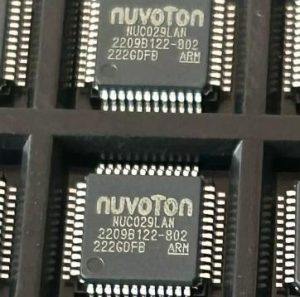
NUC029LAN

ARM Cortex-M0 MCU, 50MHz, 64KB Flash, 4KB SRAM, dual UART/SPI/I2C, LQFP-48

Brand: Nuvoton

Package: LQFP-48 (7.0 x 7.0 x 1.45 mm)

IN STOCK: 12385pcs

Cargo cycle: 3-7 Days

The minimum order is 1

MMUN2211LT1G

NPN digital transistor, R1=10kΩ R2=10kΩ, 50V, 100mA, SOT-23-3, pre-biased BRT switch

Brand: Onsemi

Package: SOT-23-3 (TO-236, SC-59)

IN STOCK: 8500pcs

Cargo cycle: 3-7 Days

The minimum order is 1

PIC32MX795F512L-80I/PF

32-bit PIC32MX MCU with Ethernet/CAN/USB, 80MHz, 512KB Flash, TQFP-100, industrial

Brand: MICROCHIP

Package: TQFP-100 (14 x 14 mm)

IN STOCK: 7912pcs

Cargo cycle: 3-7 Days

The minimum order is 1